The Gaussian beam is recognized as one of the most useful light sources. To describe the Gaussian beam, there is a mathematical formula called the paraxial Gaussian beam formula. Today, we’ll learn about this formula, including its limitations, by using the Electromagnetic Waves, Frequency Domain interface in the COMSOL Multiphysics® software. We’ll also provide further detail into a potential cause of error when utilizing this formula. In a later blog post, we’ll provide solutions to the limitations discussed here.
Gaussian Beam: The Most Useful Light Source and Its Formula
Because they can be focused to the smallest spot size of all electromagnetic beams, Gaussian beams can deliver the highest resolution for imaging, as well as the highest power density for a fixed incident power, which can be important in fields such as material processing. These qualities are why lasers are such attractive light sources. To obtain the tightest possible focus, most commercial lasers are designed to operate in the lowest transverse mode, called the Gaussian beam.
As such, it would be reasonable to want to simulate a Gaussian beam with the smallest spot size. There is a formula that predicts real Gaussian beams in experiments very well and is convenient to apply in simulation studies. However, there is a limitation attributed to using this formula. The limitation appears when you are trying to describe a Gaussian beam with a spot size near its wavelength. In other words, the formula becomes less accurate when trying to observe the most beneficial feature of the Gaussian beam in simulation. In a future blog post, we will discuss ways to simulate Gaussian beams more accurately; for the remainder of this post, we will focus exclusively on the paraxial Gaussian beam.

A schematic illustrating the converging, focusing, and diverging of a Gaussian beam.
Note: The term “Gaussian beam” can sometimes be used to describe a beam with a “Gaussian profile” or “Gaussian distribution”. When we use the term “Gaussian beam” here, it always means a “focusing” or “propagating” Gaussian beam, which includes the amplitude and the phase.
Deriving the Paraxial Gaussian Beam Formula
The paraxial Gaussian beam formula is an approximation to the Helmholtz equation derived from Maxwell’s equations. This is the first important element to note, while the other portions of our discussion will focus on how the formula is derived and what types of assumptions are made from it.
Because the laser beam is an electromagnetic beam, it satisfies the Maxwell equations. The time-harmonic assumption (the wave oscillates at a single frequency in time) changes the Maxwell equations to the frequency domain from the time domain, resulting in the monochromatic (single wavelength) Helmholtz equation. Assuming a certain polarization, it further reduces to a scalar Helmholtz equation, which is written in 2D for the out-of-plane electric field for simplicity:
where  for wavelength
  in vacuum.
The original idea of the paraxial Gaussian beam starts with approximating the scalar Helmholtz equation by factoring out the propagating factor and leaving the slowly varying function, i.e.,  , where the propagation axis is in
  and
and  is the slowly varying function. This will yield an identity
This factorization is reasonable for a wave in a laser cavity propagating along the optical axis. The next assumption is that  , which means that the envelope of the propagating wave is slow along the optical axis, and
  , which means that the variation of the wave in the optical axis is slower than that in the transverse axis. These assumptions derive an approximation to the Helmholtz equation, which is called the paraxial Helmholtz equation, i.e.,
The special solution to this paraxial Helmholtz equation gives the paraxial Gaussian beam formula. For a given waist radius  at the focus point, the slowly varying function is given by
\sqrt{\frac{w_0}{w(x)}}
\exp(-y^2/w(x)^2)
\exp(-iky^2/(2R(x)) + i\eta(x))
where  ,
,  , and
, and  are the beam radius as a function of , the radius of curvature of the wavefront, and the Gouy phase, respectively. The following definitions apply:
  ,
,  ,
,  , and
, and  .
.
Here,  is referred to as the Rayleigh range. Outside of the Rayleigh range, the Gaussian beam size becomes proportional to the distance from the focal point and the
  intensity position diverges at an approximate divergence angle of
  .
.
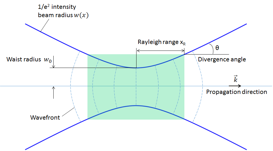
Definition of the paraxial Gaussian beam.
Note: It is important to be clear about which quantities are given and which ones are being calculated. To specify a paraxial Gaussian beam, either the waist radius
or the far-field divergence angle
must be given. These two quantities are dependent on each other through the approximate divergence angle equation. All other quantities and functions are derived from and defined by these quantities.
 must be given. These two quantities are dependent on each other through the approximate divergence angle equation. All other quantities and functions are derived from and defined by these quantities.
Simulating Paraxial Gaussian Beams in COMSOL Multiphysics®
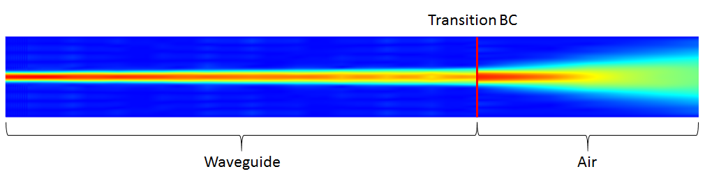
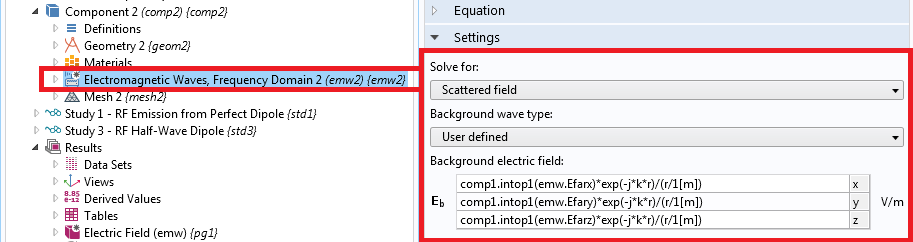
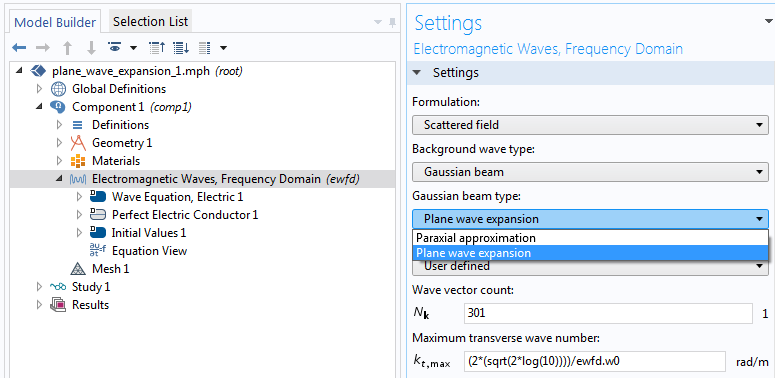
In COMSOL Multiphysics, the paraxial Gaussian beam formula is included as a built-in background field in the Electromagnetic Waves, Frequency Domain interface in the RF and Wave Optics modules. The interface features a formulation option for solving electromagnetic scattering problems, which are the Full field and the Scattered field formulations.
The paraxial Gaussian beam option will be available if the scattered field formulation is chosen, as illustrated in the screenshot below. By using this feature, you can use the paraxial Gaussian beam formula in COMSOL Multiphysics without having to type out the relatively complicated formula. Instead, you simply need to specify the waist radius, focus position, polarization, and the wave number.

Screenshot of the settings for the Gaussian beam background field.
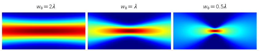
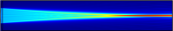
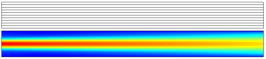
Plots showing the electric field norm of paraxial Gaussian beams with different waist radii. Note that the variable name for the background field is ewfd.Ebz.
Looking into the Limitation of the Paraxial Gaussian Beam Formula
In the scattered field formulation, the total field  is linearly decomposed into the background field
  and the scattered field
  as
as  . Since the total field must satisfy the Helmholtz equation, it follows that
  , where
  is the Laplace operator. This is the full field formulation, where COMSOL Multiphysics solves for the total field. On the other hand, this formulation can be rewritten in the form of an inhomogeneous Helmholtz equation as
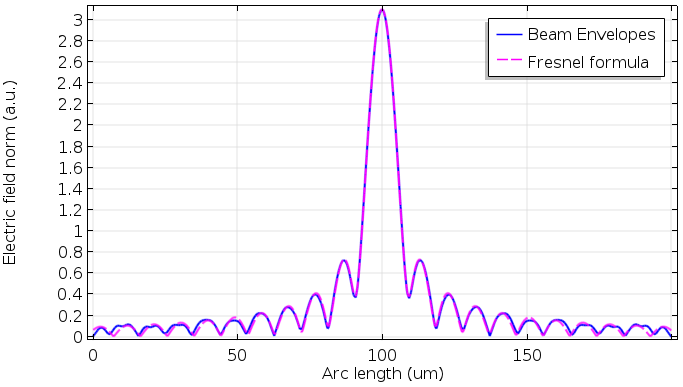
The above equation is the scattered field formulation, where COMSOL Multiphysics solves for the scattered field. This formulation can be viewed as a scattering problem with a scattering potential, which appears in the right-hand side. It is easy to understand that the scattered field will be zero if the background field satisfies the Helmholtz equation (under an approximate Sommerfeld radiation condition, such as an absorbing boundary condition) because the right-hand side is zero, aside from the numerical errors. If the background field doesn’t satisfy the Helmholtz equation, the right-hand side may leave some nonzero value, in which case the scattered field may be nonzero. This field can be regarded as an error of the background field. In other words, under certain conditions, you can qualify and quantify exactly how and by how much your background field satisfies the Helmholtz equation. Let’s now take a look at the scattered field for the example shown in the previous simulations.
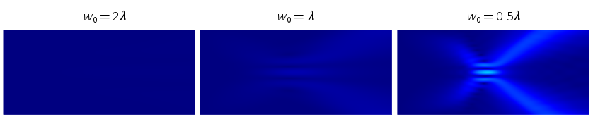
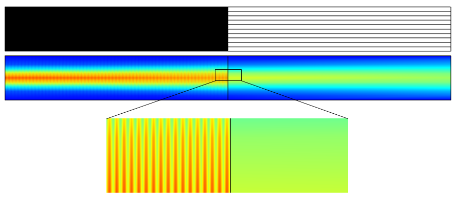
Plots showing the electric field norm of the scattered field. Note that the variable name for the scattered field is ewfd.relEz. Also note that the numerical error is contained in this error field as well as the formula’s error.
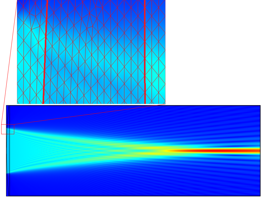
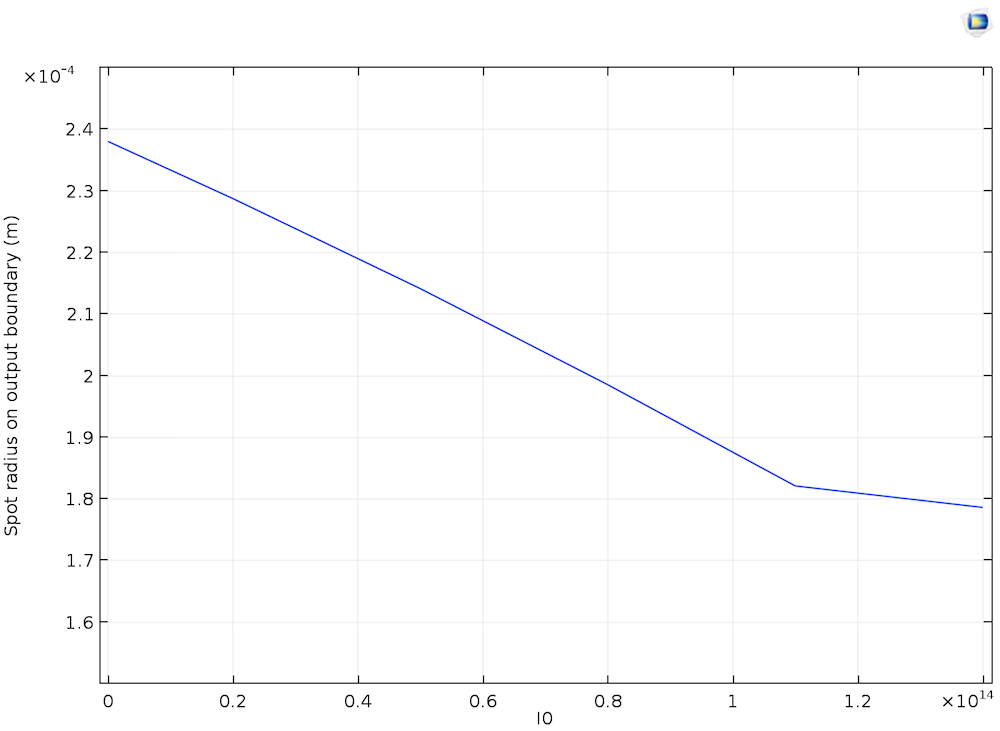
The results shown above clearly indicate that the paraxial Gaussian beam formula starts failing to be consistent with the Helmholtz equation as it’s focused more tightly. Quantitatively, the plot below may illustrate the trend more clearly. Here, the relative L2 error is defined by  , where
  stands for the computational domain, which is compared to the mesh size. As this plot suggests, we can’t expect that the paraxial Gaussian beam formula for spot sizes near or smaller than the wavelength is representative of what really happens in experiments or the behavior of real electromagnetic Gaussian beams. In the settings of the paraxial Gaussian beam formula in COMSOL Multiphysics, the default waist radius is ten times the wavelength, which is safe enough to be consistent with the Helmholtz equation. It is, however, not a “cut-off” number, as the approximation assumption is continuous. It’s up to you to decide when you need to be cautious in your use of this approximate formula.
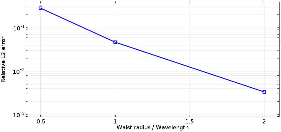
Semi-log plot comparing the relative L2 error of the scattered field with the waist size in the units of wavelength.
Checking the Validity of the Paraxial Approximation
In the above plot, we saw the relationship between the waist size and the accuracy of the paraxial approximation. Now we can check the assumptions that were discussed earlier. One of the assumptions to derive the paraxial Helmholtz equation is that the envelope function varies relatively slowly in the propagation axis, i.e., . Let’s check this condition on the x-axis. To that end, we can calculate a quantity representing the paraxiality. As the paraxial Helmholtz equation is a complex equation, let’s take a look at the real part of this quantity,  .
.
The following plot is the result of the calculation as a function of x normalized by the wavelength. (You can type it in the plot settings by using the derivative operand like d(d(A,x),x) and d(A,x), and so on.) We can see that the paraxiality condition breaks down as the waist size gets close to the wavelength. This plot indicates that the beam envelope is no longer a slowly varying one around the focus as the beam becomes fast. A different approach for seeing the same trend is shown in our Suggested Reading section.
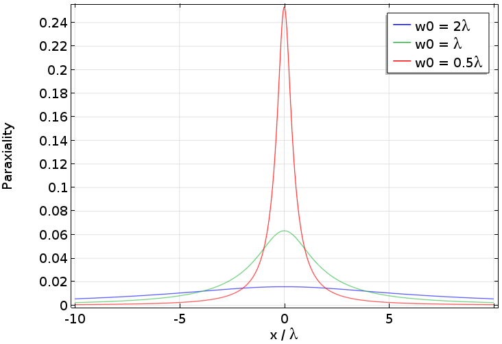
Real part of the paraxiality along the x-axis for paraxial Gaussian beams with different waist sizes.
Concluding Remarks on the Paraxial Gaussian Beam Formula
Today’s blog post has covered the fundamentals related to the paraxial Gaussian beam formula. Understanding how to effectively utilize this useful formulation requires knowledge of its limitation as well as how to determine its accuracy, both of which are elements that we have highlighted here.
There are additional approaches available for simulating the Gaussian beam in a more rigorous manner, allowing you to push through the limit of the smallest spot size. We will discuss this topic in a future blog post. Stay tuned!
Suggested Reading
- P. Vaveliuk, “Limits of the paraxial approximation in laser beams”, Optics Letters, Vol. 32, No. 8 (2007)
- Browse related topics here on the COMSOL Blog:

 is the reflection coefficient for impedance mismatch between antenna and transmission line, p is the polarization mismatch factor, λ is the wavelength, r is the distance between the antennas and is associated with the so-called
  and
and  are the angular
 , since they are incredibly useful for antenna radiation and we will use them repeatedly. Starting from the Cartesian coordinates (x, y, z), we can easily express these as follows.
 .
. and
and  , but
, but 
 .
. . For clarity, we have included two conventions here, as it is common to use
  in electrical engineering, while physicists will generally be more familiar with
  . We can then calculate the radiated power by integrating this quantity over all angles.
 and
and  for gain and directivity, respectively. Pin is the power accepted by the antenna and Prad is the total radiated power. While both quantities can be of interest, gain tends to be the more practical of these two as it accounts for material loss in the antenna. Because of its prevalence and usefulness, we also include the definition of gain (in a given direction) from “IEEE Standard Definitions of Terms for Antennas”, which is: “The ratio of the radiation intensity, in a given direction, to the radiation intensity that would be obtained if the power accepted by the antenna were radiated isotropically.”
 , where
  is the reflection coefficient from transmission line theory, Zc is the characteristic impedance of the transmission line, and Z is the impedance of the antenna.
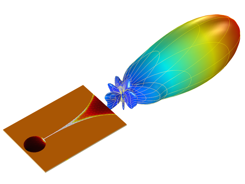
 , of the antenna by the incident power flux and accounting for impedance mismatch in the line, yielding
  . As you may expect, this bears a striking similarity to several terms of the Friis transmission equation.
 is the dipole moment of the radiation source (not to be confused with the polarization mismatch) and k is the wave vector for the medium.
 , a fact that we will take advantage of.
 , where Z0 is the impedance of free space and c is the speed of light. The maximum gain is 1.5 and is isotropic in the plane normal to the dipole moment (e.g., the xy-plane for a dipole in
  ).
). in Coulomb*meters (Cm). In antenna and engineering texts, it is common to specify an infinitesimal current dipole in Ampere*meters (Am). COMSOL Multiphysics follows the engineering convention. The two definitions are related by a time derivative, so for a COMSOL software implementation, the dipole moment
  to obtain the infinitesimal current dipole.
 and a directivity of
  . It is worth mentioning that the antenna impedance will change from these values for an antenna of finite radius. The receiving antenna we use here has a length of 0.47 λ and a length-to-diameter ratio of 100. With these values, we simulate an impedance of
  , which is close to the infinitely thin value and also agrees reasonably well with
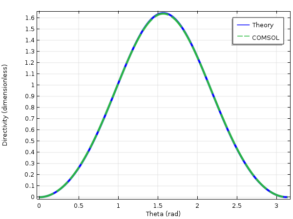
 , but not radial position. The decrease in field strength is solely governed by the 1/r term. There are also variables emw.Efarphi and emw.Efartheta, which are for the scattering amplitude in spherical coordinates.
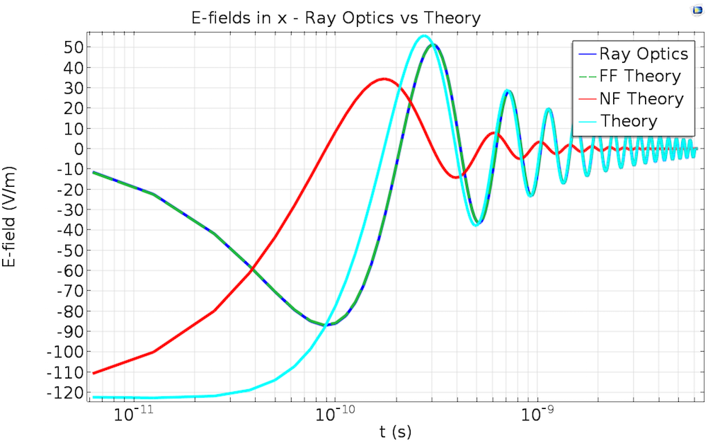
 . For comparison, we have included the Far-Field Domain node, the full theory, as well as the near- and far-field terms individually. The fields are evaluated along an arbitrary cut line. As you can see, there is overlap between the Far-Field Domain node and the far-field theory plots, and they agree with the full theory as the distance from the antenna increases. This is because the Far-Field Domain node will only account for radiation that goes like 1/r, and so the agreement improves with increasing distance as the contribution of the 1/r2 and 1/r3 terms go to zero. In other words, the Far-Field Domain node is correct in the far field, which you probably would have guessed from the name.
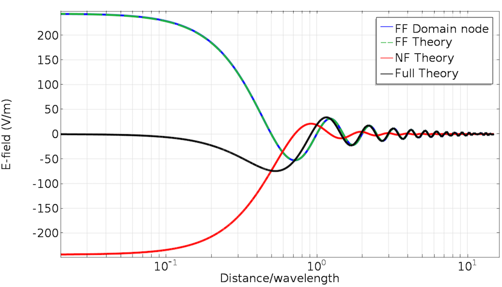
 for
for 
 , as the point we are actually interested in. In the image below, we show the point where we would like to evaluate the scattering amplitude.
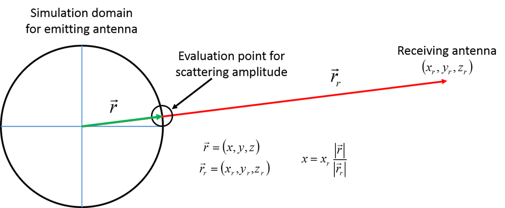
 and sim_r =
  .
. 
 , as the point in which we are actually interested.
 represent a vector in component 1, a vector in component 2, and the offset between the antennas, respectively.
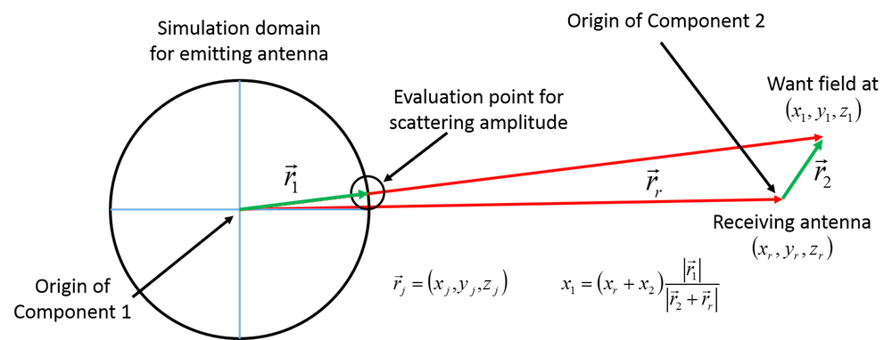
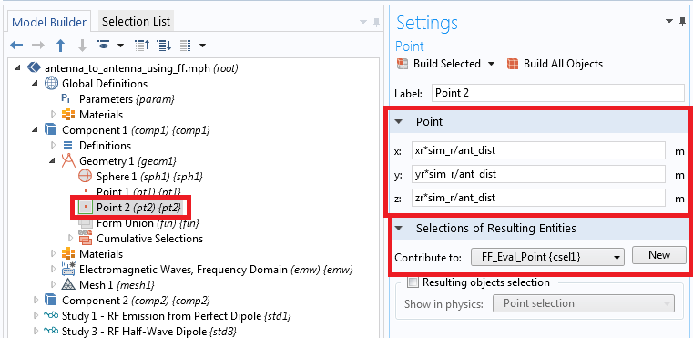
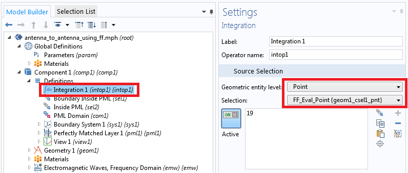
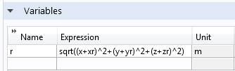
 , which requires calculating the scattering amplitude at
  . The complication, of course, is that each point in the domain around the receiving antenna (each vector
  ) will have its own evaluation location
  , with corresponding equations for y and z. The operator is defined in component 1, so the source will be defined in that component. It will be called from component 2, so the x, y, z in the following expressions refer to x2, y2, z2 in the above figure.
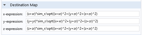
 variable specifies the correct spatial intensity distribution for the rays (as antennas generally do not emit uniformly) and is calculated according to
  , where Z is the impedance of the medium.
 is the radius of the spherical boundary that we are launching the rays from and will correctly initialize the curvature of the ray wavefront.
 to specify the initial principal curvature direction. This ensures that the correct polarization orientation is imparted to the rays. The wavefront shape here must be set to Ellipsoid — even though the surface is technically a sphere — because we need to be able to specify a preferred direction for polarization. If we choose Spherical, then each orientation is degenerate and we cannot make that specification.


 plane at
  . The diffracted electric field in the
  plane at the distance
  from the diffracting aperture is calculated as
 is the wavelength and
  account for the electric field at the
  .
.  . So, the sign of the quadratic phase function is negative.
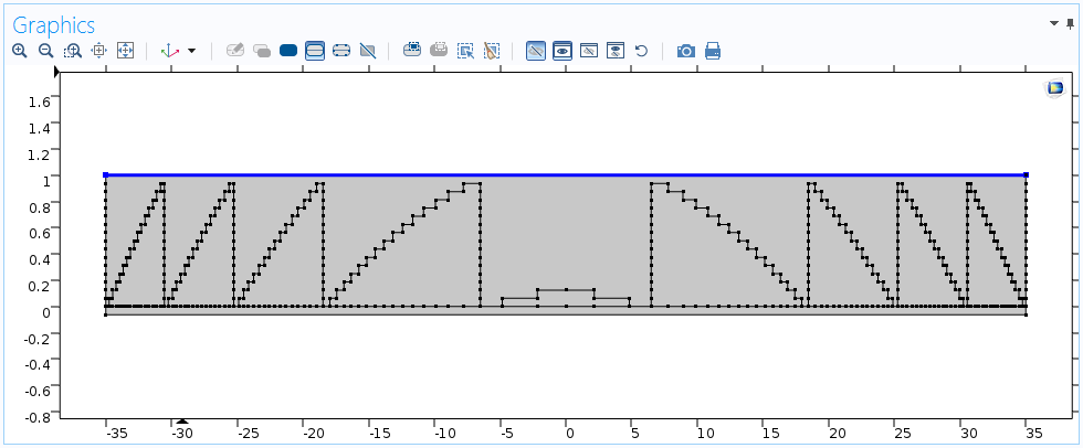
 along the lens height, where m is an integer and n is the refractive index of the lens material. This is called an mth-order Fresnel lens.
 (roughly speaking and under the paraxial approximation). Because of this, the folded lens fundamentally reproduces the same wavefront in the far field and behaves like the original unfolded lens. The main difference is the diffraction effect. Regular lenses basically don’t show any diffraction (if there is no vignetting by a hard aperture), while Fresnel lenses always show small diffraction patterns around the main spot due to the surface discontinuities and internal reflections.
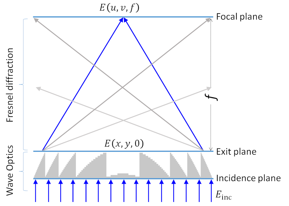
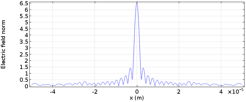
 is incident on the incidence plane. At the exit plane at
  . This process can be easily modeled and simulated by the Wave Optics, Frequency Domain interface. Then, we calculate the field
  at the focal plane at
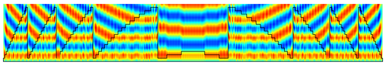
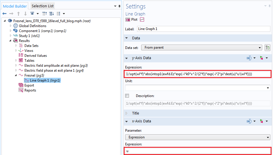
 in the focal plane. We then relate it to the source data set, as seen in the figure below. Then, we define an integration operator


 and
and  terminology (Ref. 2), where x and y depict the direction of polarization and p and q depict the number of maxima in the x- and y-coordinates.
 “landscape” (as shown below). The “winds” (polarization) are along ±x direction, and you encounter two distinct peaks when traveling from the -x to +x direction. When you move from the -y to +y direction, you observe both of the peaks simultaneously.


 and
and  . Middle row, left to right:
  and
and  . Bottom row, left to right:
  . The arrow plot represents the electric field; contour and surface plot represent out-of-plane power flow (red is high and blue is low magnitude).
 xx,
xx,  , it is known as a biaxial crystal.
 and nyy =
  .
.
 with the x-axis, the diagonal components


 with the y-axis, the diagonal components

 is the dependent variable that the interface solves for, called the envelope function.
 to the phase, i.e.,
 , where
  for wavelength
  = 1 um, it propagates in a rectangular domain of 20 um length. (We intentionally use a short domain for illustrative purposes.)
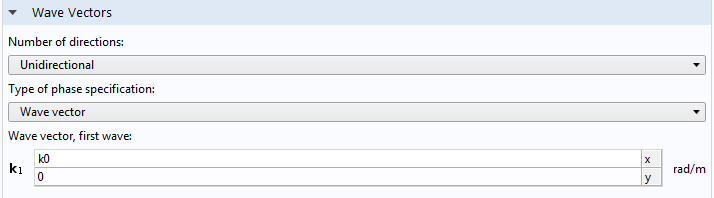
 , knowing that the correct phase function is
  or the wave vector is
  a priori. Substituting the phase function in the second equation, we inversely get
  , the constant function.
 ,
,  . Here, we can see that we get the correct envelope function if we give the exact phase function, constant one, for any number of meshes, as expected. For confirmation purposes, the phase of
  ,
, 
 instead of the exact
 . This results in
  , which is no longer constant one. This is a wave with a wavelength of
  = 20 um, which is called the beat wavelength.
  . The plots for the lower resolutions still show an approximate solution of the envelope function. This is as expected for finite element simulations: coarser mesh gives more approximate results.
 .
.  , which is the correct fast field!
 instead of
  . In this case, the wave number is correct but the wave vector is off. This time, the beating takes place in 2D.
 and the envelope function is now calculated to be
  , which is a tilted wave propagating to direction
  , with the beat wave number
  and the beat wavelength
  .
. . (Note that we have to give the corresponding wrong boundary condition because our phase guess is wrong.)
  is computed to be constant one. These results are consistent with the 1D example case.
 , computed for different mesh sizes. The color range represents the values from -1 to 1.
 , which is not accurate at all. In the region before the lens, there is a reflection, which creates an interference. In the lens, there are multiple reflections. After the lens, the phase is spherical so that the beam focuses into a spot. So this phase function is far different from what is happening around the lens. Still, we have a clue. If we plot
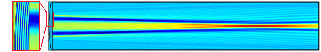
 in front of the lens. To prove this, we can perform the same calculations as in the previous examples. The finest beat wavelength is due to the interference between the incident beam and reflected beam, but we can ignore this because it doesn’t contribute to the forward propagation. We can see that the mesh doesn’t resolve the beating before the lens, but let’s ignore this for now.
 for the backward beam and
  for the forward beam for n = 1.5, which we can also prove in the same way as the previous examples. Again, we ignore the backward beam. In the plot, what’s visible is the
 , which is equal to
  . This makes it easier to mesh the lens domain.
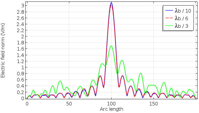
 is the vacuum permittivity, and
  is the isotropic susceptibility.
 ) of the medium and, using a power series expansion, as follows:
 is the ith-order susceptibility.
  ) deals with the change in refractive index due to the dipole oscillation of the bound and free carriers, such as electrons. Hendrik Lorentz originally came up with the idea of creating a mathematical oscillator model that can relate the dipole oscillation of bound electrons to the susceptibility of the material. Paul Drude originated the idea of oscillation within semiconductors, which deals with free carriers within the material. After combining the effects of bound and free carriers, the new model was called the Drude-Lorentz model.
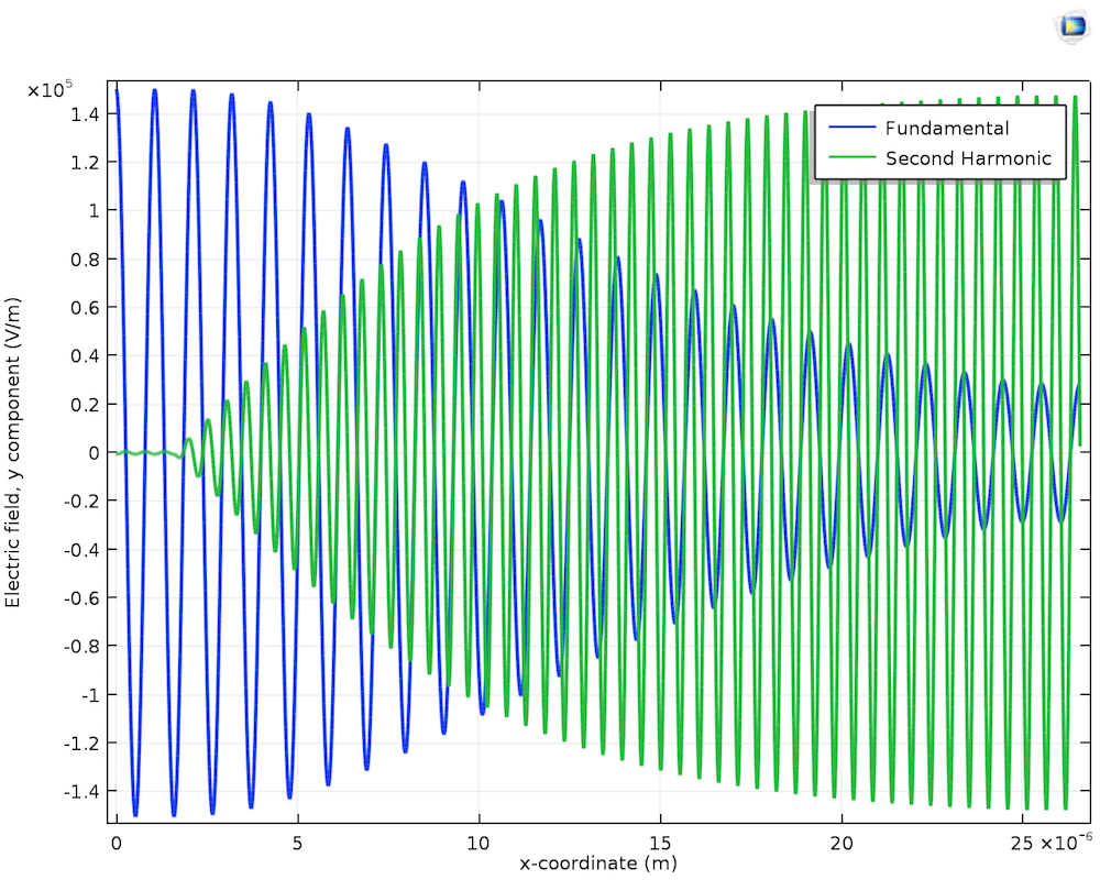
 ). When a monochromatic beam of light is introduced and passes through such a nonlinear crystal, not only does the output frequency spectrum show the original frequency (ω), but it also indicates the second-order harmonic frequency (2ω). Hence, this phenomenon is called second-harmonic generation (SHG).
 ,
,  is the nonlinear coefficient, and Ez is the z-component of the electric field.
  , and that of the second interface,
  , can be defined as the following:
  is the y-component of the electric field at the fundamental frequency, and
  is the y-component of the electric field at the second-harmonic frequency.
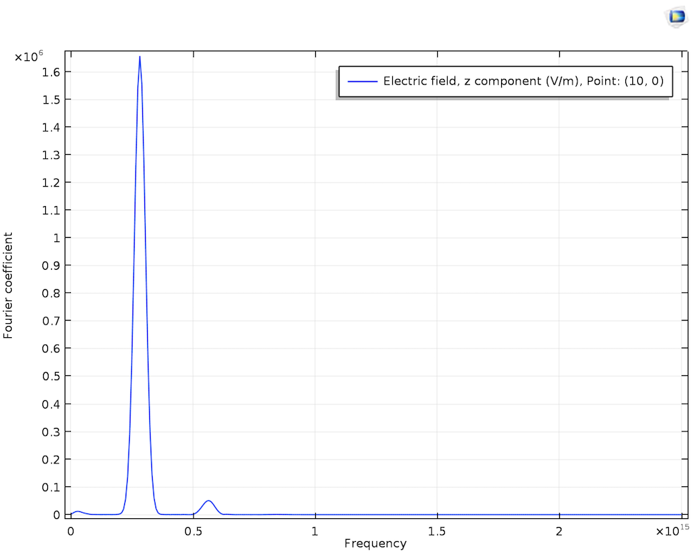
 ) display phenomena such as the optical Kerr effect, self-phase modulation, cross-phase modulation, third-harmonic generation, and four-wave mixing. To illustrate
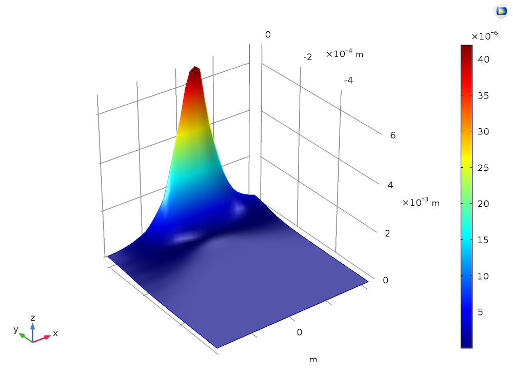


 for our choice of polarization:
 .
. is an arbitrary function.
 for real
  and
and  . (For complex
  satisfies Helmholtz’s equation by direct substitution.
 , we can set
  and
and  and rewrite the above equation as:
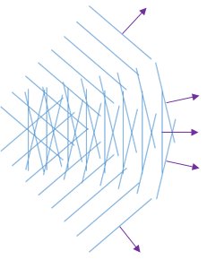
 that satisfies the boundary conditions. By assuming that the profile of the transverse field (perpendicular to the propagating direction, i.e., optical axis) is also a Gaussian shape (see
  , where
  is the spectrum width.
 . For example, for a slow Gaussian beam, the angular spectrum is narrow. A plane wave, on the other hand, is the extreme case where the angular spectrum function is a delta function. For a fast Gaussian beam, the angular spectrum is wider, and vice versa.
 :
:
 . This integral bound can be the maximum
  for the smallest possible spot size and can be more shallow for slower beams, depending on how fast the Gaussian beam is. You need more angled plane waves with a larger transverse wave number to represent faster (more focused) beams.
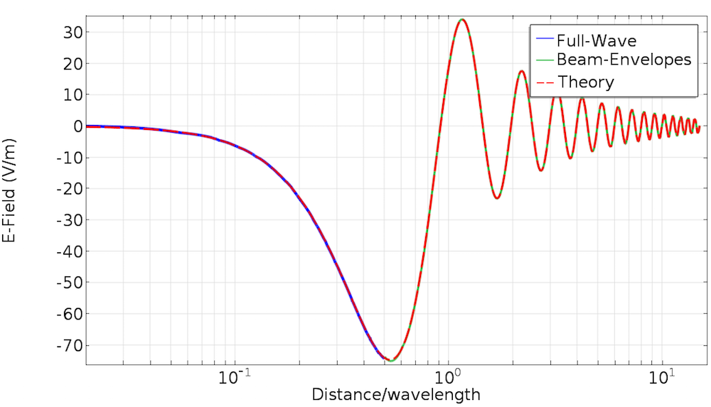
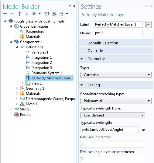
 , which is considerably nonparaxial. As in the previous blog post, the simulation is done with the Scattered Field formulation and the domain is surrounded by a perfectly matched layer (PML). This way, the scattered field represents the error from the exact Helmholtz solution.


 and
and  are the electric and magnetic field intensity, respectively;
  and
and  are the electric and magnetic flux density, respectively; and
  and
and  are the electric charge density and electric conduction current density, respectively.
 is the permittivity and
  is the permeability of the medium.
  is the outward normal from medium 2 and
  and
and  the surface electric charge density and surface current density, respectively.
 and defining
  , equations
  always holds. Poisson’s equation is expressed as:
 and defining
  , equations
  always holds.
 operator. In fact, other situations, such as
  is the frequency and
  is the imaginary unit.
 can be approximated with the linear function
  as
as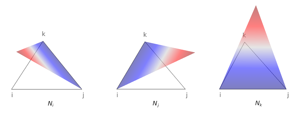
 . The electric field close to the boundary
  to both sides of equation
  gives
gives being the boundary of the domain and
  the normal vector oriented away from the domain.
 vanishes on the boundary. To clearly see how it works, it is convenient to rewrite equation
  .
. . However, it is complicated to implement the boundary conditions, especially for irregular boundaries. Even so, the results could be spurious, since the Lagrange element would enforce each component
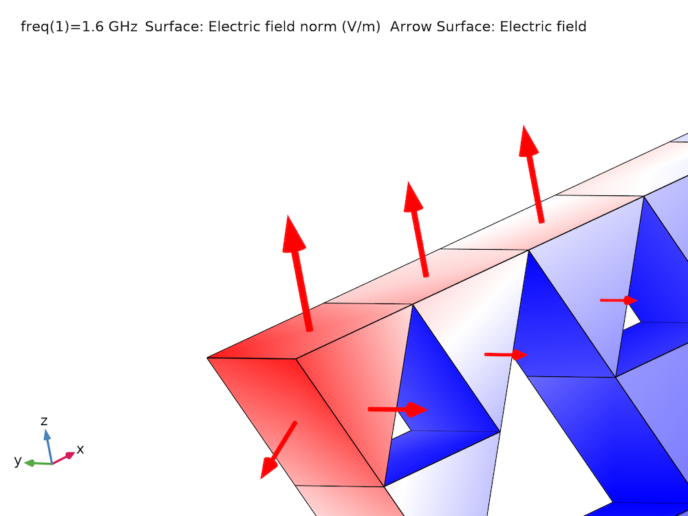
 space (
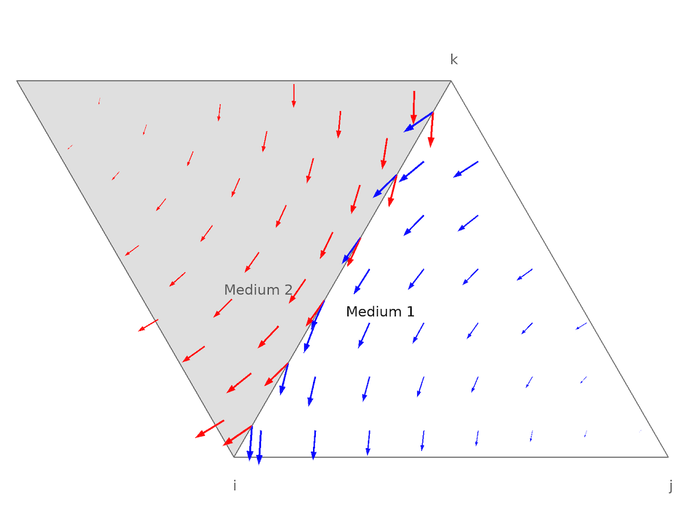
 to both sides of equation
  . In the Magnetic Fields interface, the default boundary condition is Magnetic Insulation, which constrains the tangential magnetic vector potential to be zero; i.e.,
  . These boundary conditions could be easily considered by the FEM using pointwise constraints since the unknowns are exactly the tangential fields on the boundary. There are other advantages of using curl elements, such as eliminating spurious solutions, especially for solving electromagnetic wave problems (
 , where
  is the element size, while using linear Lagrange elements, the local errors converge at
  (
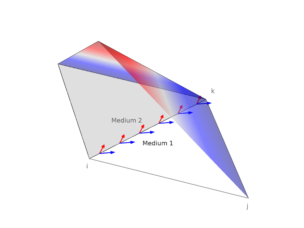
( along edge
  and any direction parallel to edge
  are constants depending on the coordinates of the element only.
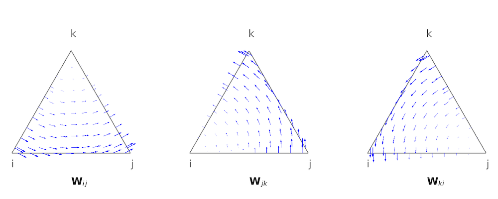
 component of
  axis. The accuracy of the spatial derivatives of each component would be significantly different. For this reason, when postprocessing curl elements, the higher-order spatial derivatives of the fields are not available. Equation
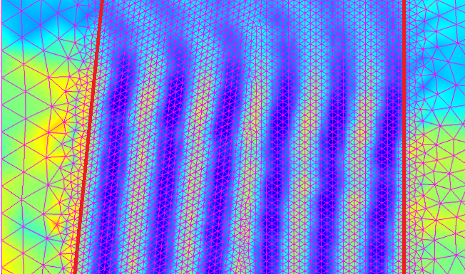
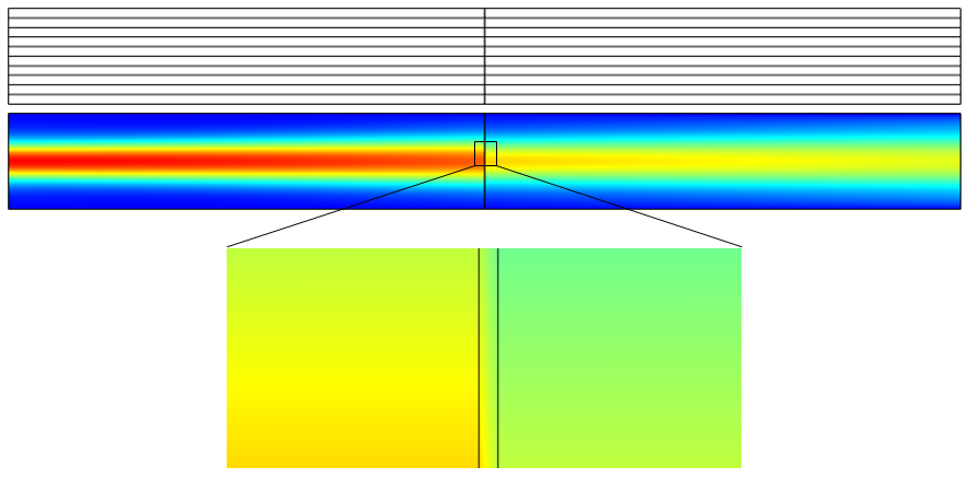
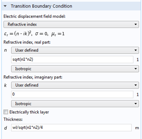
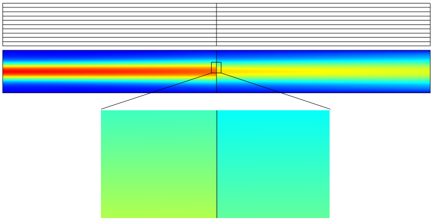
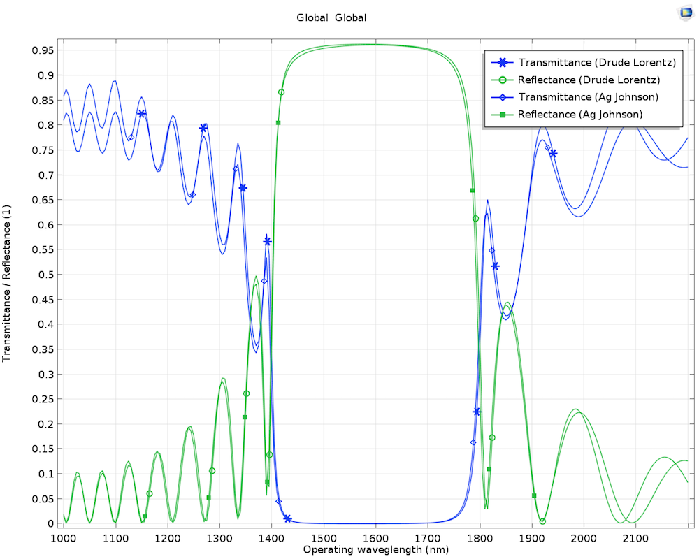
 , where
  and
and  are the index for each material sandwiching the film and with the thickness of
  , where
  is the vacuum wavelength. With this film, the reflectance becomes zero at