Quantcast
Channel: Wave Optics – COMSOL Blog
Viewing all 46 articles
Browse latest View live

Modeling Electromagnetic Waves and Periodic Structures

$
0
0

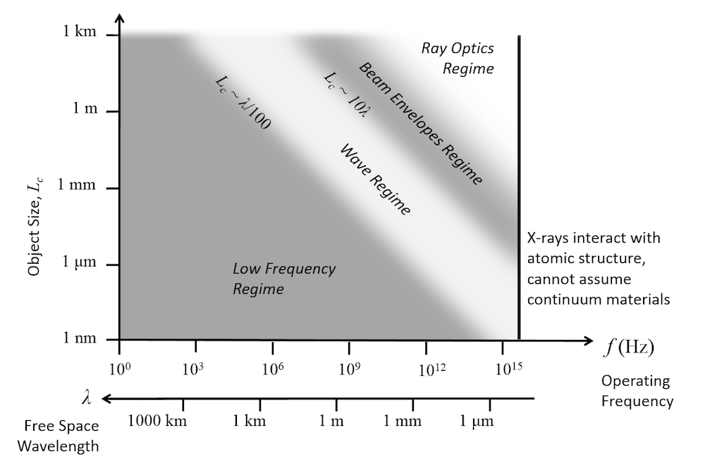
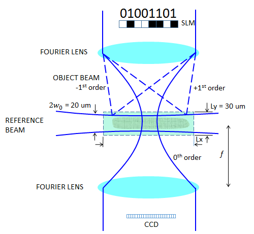
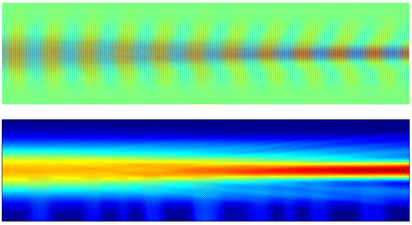
We often want to model an electromagnetic wave (light, microwaves) incident upon periodic structures, such as diffraction gratings, metamaterials, or frequency selective surfaces. This can be done using the RF or Wave Optics modules from the COMSOL product suite. Both modules provide Floquet periodic boundary conditions and periodic ports and compute the reflected and transmitted diffraction orders as a function of incident angles and wavelength. This blog post introduces the concepts behind this type of analysis and walks through the set-up of such problems.

The Scenario

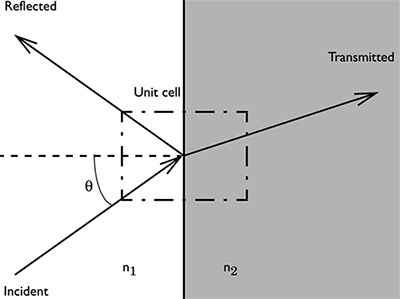
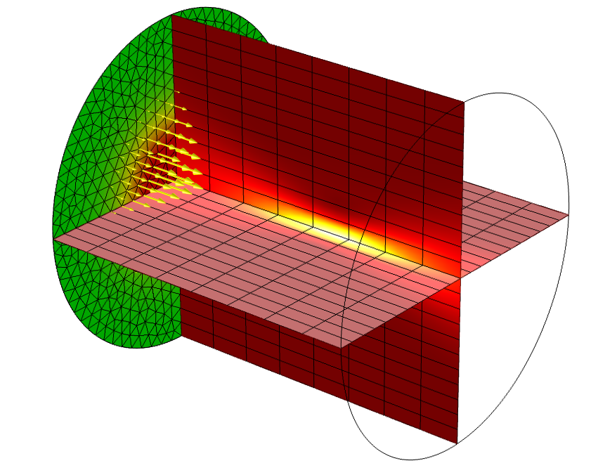
First, let’s consider a parallelepided volume of free space representing a periodically repeating unit cell with a plane wave passing through it at an angle, as shown below:

a diagram of a plane wave passing through a periodically repeating unit cell

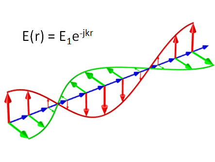
The incident wavevector, \bf{k}, has component magnitudes: k_x = k_0 \sin(\alpha_1) \cos(\alpha_2), k_y = k_0 \sin(\alpha_1) \sin(\alpha_2), and k_z = k_0 \cos(\alpha_1) in the global coordinate system. This problem can be modeled by using Periodic boundary conditions on the sides of the domain and Port boundary conditions at the top and bottom. The most complex part of the problem set-up is defining the direction and polarization of the incoming and outgoing wave.

Defining the Wave Direction

Although the COMSOL software is flexible enough to allow any definition of base coordinate system, in this posting, we will pick one and use it throughout. The direction of the incident light is defined by two angles, \alpha_1 and \alpha_2; and two vectors, \bf{n}, the outward pointing normal of the modeling space and \bf{a_1}, a vector in the plane of incidence. The convention we choose here is to align \bf{a_1} to the global x-axis and align \bf{n} with the global z-axis. Thus, the angle between the wavevector of the incoming wave and the global z-axis is \alpha_1, the elevation angle of incidence, where -\pi/2 > \alpha_1 > \pi/2 with \alpha_1 = 0, meaning normal incidence. The angle between the incident wavevector and the global x-axis is the azimuthal angle of incidence, \alpha_2, which lies in the range, -\pi/2 > \alpha_2 \geq \pi/2. As a consequence of this definition, positive values of both \alpha_1 and \alpha_2 imply that the wave is traveling in the positive x- and y-direction.

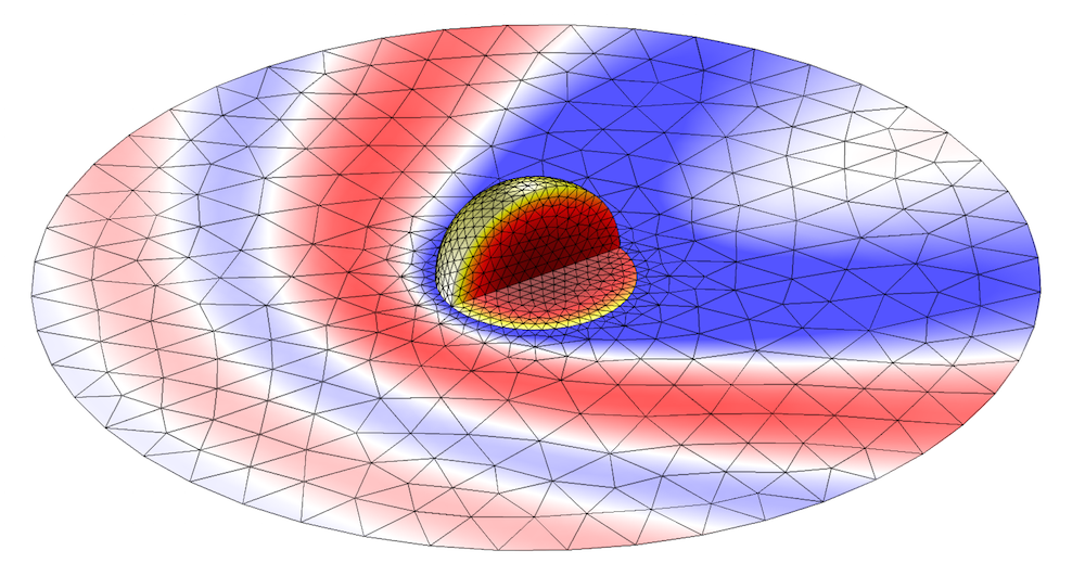
To use the above definition of direction of incidence, we need to specify the \bf{a_1} vector. This is done by picking a Periodic Port Reference Point, which must be one of the corner points of the incident port. The software uses the in-plane edges coming out of this point to define two vectors, \bf{a_1} and \bf{a_2}, such that \bf{a_1 \times a_2 = n}. In the figure below, we can see the four cases of \bf{a_1} and \bf{a_2} that satisfy this condition. Thus, the Periodic Port Reference Point on the incoming side port should be the point at the bottom left of the x-y plane, when looking down the z-axis and the surface. By choosing this point, the \bf{a_1} vector becomes aligned with the global x-axis.

A diagram of the Periodic Port Reference Point of a periodically repeating unit cell

Now that \bf{a_1} and \bf{a_2} have been defined on the incident side due to the choice of the Periodic Port Reference Point, the port on the outgoing side of the modeling domain must also be defined. The normal vector, \bf{n}, points in the opposite direction, hence the choice of the Periodic Port Reference Point must be adjusted. None of the four corner points will give a set of \bf{a_1} and \bf{a_2} that align with the vectors on the incident side, so we must choose one of the four points and adjust our definitions of \alpha_1 and \alpha_2. By choosing a periodic port reference point on the output side that is diametrically opposite the point chosen on the input side and applying a \pi/2 rotation to \alpha_2, the direction of \bf{a_1} is rotated to \bf{a_1'}, which points in the opposite direction of \bf{a_1} on the incident side. As a consequence of this rotation, \alpha_1 and \alpha_2 are switched in sign on the output side of the modeling domain.

A diagram of the periodic port reference point on the output side of a periodically repeating unit cell

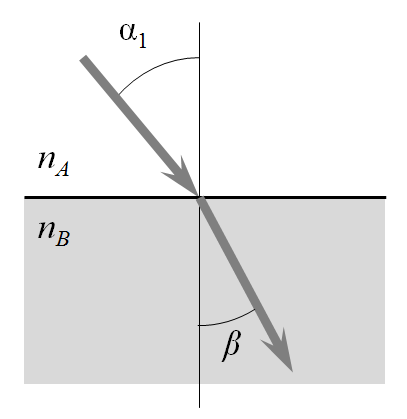
Next, consider a modeling domain representing a dielectric half-space with a refractive index contrast between the input and output port sides that causes the wave to change direction, as shown below. From Snell’s law, we know that the angle of refraction is \beta=\arcsin \left( n_A\sin(\alpha_1)/n_B \right). This lets us compute the direction of the wavevector at the output port. Also, note that this relationship holds even if there are additional layers of dielectric sandwiched between the two half-spaces.

A diagram representing Snell's Law

In summary, to define the direction of a plane wave traveling through a unit cell, we first need to choose two points, the Periodic Port Reference Points, which are diametrically opposite on the input and output sides. These points define the vectors \bf{a_1} and \bf{a_2}. As a consequence, \alpha_1 and \alpha_2 on the input side can be defined with respect to the global coordinate system. On the output side, the direction angles become: \alpha_{1,out} = -\arcsin \left( n_A\sin(\alpha_1)/n_B \right) and \alpha_{2,out}=-\alpha_2 + \pi/2.

Defining the Polarization

The incoming plane wave can be in one of two polarizations, with either the electric or the magnetic field parallel to the x-y plane. All other polarizations, such as circular or elliptical, can be constructed from a linear combination of these two. The figure below shows the case of \alpha_2 = 0, with the magnetic field parallel to the x-y plane. For the case of \alpha_2 = 0, the magnetic field amplitude at the input and output ports is (0,1,0) in the global coordinate system. As the beam is rotated such that \alpha_2 \ne 0, the magnetic field amplitude becomes (\sin(\alpha_2), \cos(\alpha_2),0). For the orthogonal polarization, the electric field magnitude at the input can be defined similarly. At the output port, the field components in the x-y plane can be defined in the same way.

A diagram showing polarization of a magnetic field parallel to the x-y plane of a periodically repeating unit cell

So far, we’ve seen how to define the direction and polarization of a plane wave that is propagating through a unit cell around a dielectric interface. You can see an example model of this in the Model Gallery that demonstrates an agreement with the analytically derived Fresnel Equations.

Defining the Diffraction Orders

Next, let’s examine what happens when we introduce a structure with periodicity into the modeling domain. Consider a plane wave with \alpha_1, \alpha_2 \ne 0 incident upon a periodic structure as shown below. If the wavelength is sufficiently short compared to the grating spacing, one or several diffraction orders can be present. To understand these diffraction orders, we must look at the plane defined by the \bf{n} and \bf{k} vectors as well as in the plane defined by the \bf{n} and \bf{k \times n} vectors.

A diagram showing diffraction of a plane wave

First, looking normal to the plane defined by \bf{n} and \bf{k}, we see that there can be a transmitted 0th order mode with direction defined by Snell’s law as described above. There is also a 0th order reflected component. There also may be some absorption in the structure, but that is not pictured here. The figure below shows only the 0th order transmitted mode. The spacing, d, is the periodicity in the plane defined by the \bf{n} and \bf{k} vectors.

A diagram representing the zeroth order transmitted mode

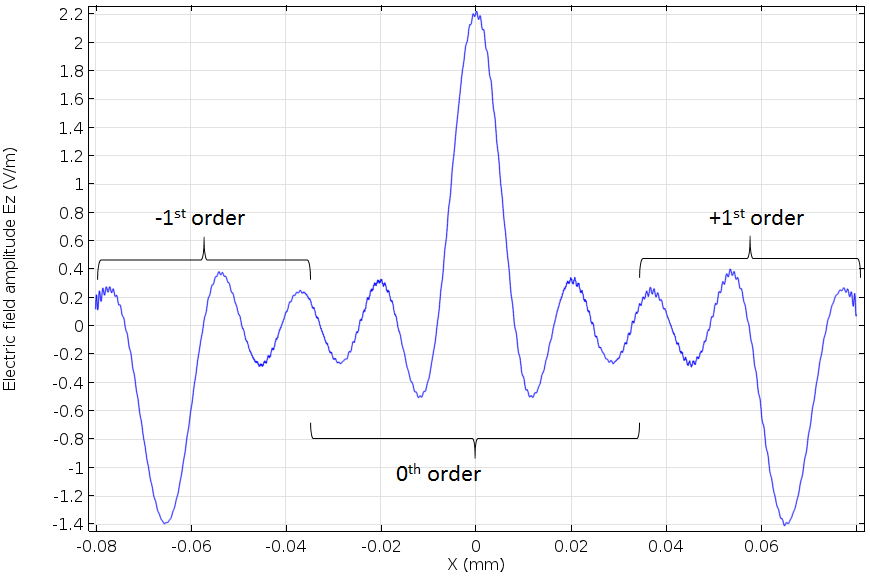
For short enough wavelengths, there can also be higher-order diffracted modes. These are shown in the figure below, for the m=\pm1 cases.

A diagram showing higher-order diffracted modes of short wavelengths

The condition for the existence of these modes is that:

m\lambda_0 = d(n_B \sin \beta_m - n_A \sin \alpha_1)

for: m=0,\pm 1, \pm 2,

For m=0 , this reduces to Snell’s law, as above. For \beta_{m\ne0}, if the difference in path lengths equals an integer number of wavelengths in vacuum, then there is constructive interference and a beam of order m is diffracted by angle \beta_{m}. Note that there need not be equal numbers of positive and negative m-orders.

Next, we look along the plane defined by the \bf{n} and \bf{k} vectors. That is, we rotate our viewpoint around the z-axis such that the incident wavevector appears to be coming in normally to the surface. The diffraction into this plane are indexed as the n-order beams. Note that the periodic spacing, w, will be different in this plane and that there will always be equal numbers of positive and negative n-orders.

A diagram showing diffraction a along a plane defined by the n and k vectors

COMSOL will automatically compute these m,n \ne 0 order modes during the set-up of a Periodic Port and define listener ports so that it is possible to evaluate how much energy gets diffracted into each mode.

Last, we must consider that the wave may experience a rotation of its polarization as it gets diffracted. Thus, each diffracted order consists of two orthogonal polarizations, the In-plane vector and Out-of-plane vector components. Looking at the plane defined by \bf{n} and the diffracted wavevector \bf{k_D}, the diffracted field can have two components. The Out-of-plane vector component is the diffracted beam that is polarized out of the plane of diffraction (the plane defined by \bf{n} and \bf{k}), while the In-plane vector component has the orthogonal polarization. Thus, if the In-plane vector component is non-zero for a particular diffraction order, this means that the incoming wave experiences a rotation of polarization as it is diffracted. Similar definitions hold for the n \ne 0 order modes.

A diagram showing the in-plane vector and out-of-plane vector of a diffracted wave

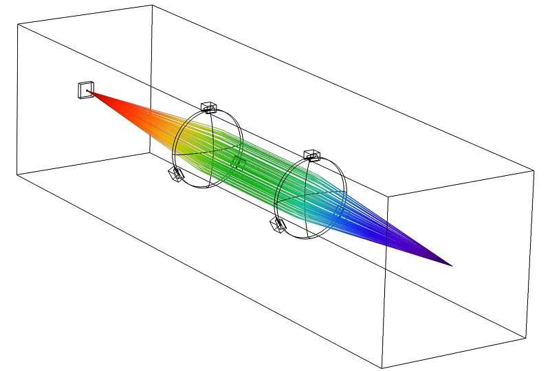
Consider a periodic structure on a dielectric substrate. As the incident beam comes in at \alpha_1, \alpha_2 \ne 0 and there are higher diffracted orders, the visualization of all of the diffracted orders can become quite involved. In the figure below, the incoming plane wave direction is shown as a yellow vector. The n=0 diffracted orders are shown as blue arrows for diffraction in the positive z-direction and cyan arrows for diffraction into the negative z-direction. Diffraction into the n \ne 0 order modes are shown as red and magenta for the positive and negative directions. There can be diffraction into each of these directions and the diffracted wave can be polarized either in or out of the plane of diffraction. The plane of diffraction itself is visualized as a circular arc. Note that the plane of diffraction for the n \ne 0 modes is different in the positive and negative z-direction.

A visualization of all of the diffracted orders on a dielectric substrate

All of the ports are automatically set up when defining a periodic structure in 3D. They capture these various diffracted orders and can compute the fields and relative phase in each order. Understanding the meaning and interpretation of these ports is helpful when modeling periodic structures.


Benchmark Model Results Agree with Fresnel Equations

$
0
0

Have you ever wondered why boaters wear polarized sunglasses? It’s because sunlight reflecting off the water is primarily polarized in one direction, and polarized sunglasses will block this component of the reflected light, thus reducing glare. To understand why this is, we can use COMSOL software. This example solves the governing Maxwell’s equations using the RF Module or Wave Optics Module to simulate light incident at an angle upon a dielectric medium, and the solution shows agreement with analytic solutions.

When Light Hits a Dielectric Medium

Sunlight is essentially incoherent light; it is composed of many wavelengths and varying polarizations. However, we can assume linearity of the electromagnetic fields, so any polarization of light can be treated as the sum of two orthogonal polarizations — one that has the electric field polarized parallel to the plane of the interface, and the other that has the magnetic field parallel to the plane of the interface.

When a ray of light (an electromagnetic wave) propagating through free space hits a dielectric medium, part of the light will be transmitted and part will be reflected. The fraction of the light that is reflected or transmitted is dependent upon the angle of incidence, the permittivity of the dielectric, and the polarization. This can also be described by the Fresnel equations, which are an analytic solution to Maxwell’s equations.

Model of wave propagation
Schematic showing light incident upon a dielectric interface. The angle of incidence is denoted by θ. Part of the light will be transmitted and part will be reflected.

Instead of solving the Fresnel equations, we can build a COMSOL model to simulate an infinite plane wave of light incident upon a dielectric medium. Using either the RF Module or the Wave Optics Module, we can build a unit cell describing a small region around the dielectric interface. We solve the full Maxwell’s equations in the unit cell, with periodic boundary conditions and ports to truncate the modeling domain.

Fresnel Equations and COMSOL Model Results Agree

Let’s take a look at the results of our benchmark model, which solves for two orthogonal polarizations of light and computes the reflection and transmission coefficients with respect to incident angle.

Electric field and power flow in the y-direction

The electric field in the y-direction (surface slice plot) and the power flow (arrow plot).

The magnetic field and power flow in the y-direction

The magnetic field in the y-direction and the power flow. Both are shown for θ = 70°.

Comparing reflectance and transmittance for electric field incidence
Comparing results for reflectance and transmittance for magnetic field incidence

Comparing COMSOL model results with analytic solution for reflectance and transmittance for electric field incidence (left) and magnetic field incidence (right).

As you can see in the above plots, the benchmark model results agree with the analytic solution. We can also see that different polarizations of light will reflect differently off of an air-dielectric interface, and this tells us why polarized sunglasses are popular with boaters!

Further Reading

Optimizing Mach-Zehnder Modulator Designs with COMSOL Software

$
0
0

The Mach-Zehnder modulator is a type of optical modulator used for communication applications. To understand how it works and how to optimize its design, you can use the COMSOL simulation software.

How the Modulator Works, Briefly

The modulator controls the amplitude of an optical wave as it passes through the device. Its name stems from the use of a Mach-Zehnder interferometer located between two 50/50 directional couplers. By applying a voltage across one of the two interferometer arms, we can alter the refractive index of the waveguide material and trigger a phase shift of the propagating electromagnetic wave. Then, the two waves combine again in a second directional coupler, and thanks to the phase difference created by the voltage, we get an amplitude modulation.

Alternatively, if the modulator’s input and output ports are all connected to other waveguides, the device can act as a spatial switch instead of an amplitude modulator. In that case, we can tune the voltage so the light switches between the two output ports.

Mach-Zehnder modulator with an applied voltage
A Mach-Zehnder modulator with an applied voltage on one of the interferometer arms.

Designing a Mach-Zehnder Modulator

Suppose we want to design a Mach-Zehnder modulator. We need it to produce low loss, give us a 50/50 split of power through the two output arms, and be used as a spatial switch.

To determine the ideal design of the device, we turn to COMSOL Multiphysics and the Wave Optics Module.

Low Loss

In order to meet the general requirement of keeping the overall size of the device small, we need to find the smallest possible bend radius that also provides low loss. To figure this out, we can plot the total modal transmission over the increasing bend radius of the curvature. Doing so shows us that a minimum bend radius of 2.5 millimeters gives us an acceptable 2% loss (the plot depicts a total modal transmission of 98%). We can also confirm our results by generating an electric field norm plot.
Plot of the total modal transmission
Plotting the total modal transmission over the bend radius of curvature in meters.

50/50 Split

Next, we have to find how long the coupler needs to be in order to give us our desired 50/50 split of incident power through the two output arms of the Mach-Zehnder interferometer. This can be achieved by monitoring the power difference in the two arms and sweeping the length of the coupler. If we plot the results of the parameter sweep, we will see that a coupler length of 380 μm will ensure a 50/50 split of power between the arms. Again, we can confirm our results with an electric field norm plot.

Here’s what the plot will look like:
Electric field norm plot of two interferometer waveguide arms
Electric field norm plot confirming that the power is close to equal in the two interferometer waveguide arms for a 380 micrometer long directional coupler. Gemetry is scaled by a factor of 80 in the y-direction.

Spatial Switch

Finally, we want to confirm that we can use the device as a spatial switch if we have a scenario where all the input and output ports are connected to other fibers or waveguides. In other words, we need to check that the wave can be switched between two output ports by applying a voltage across the waveguide in one of the arms and then tuning it. The below plot shows that we can, indeed, switch the output port by tuning the voltage:

Graph of the transmission output waveguides versus the applied voltage
Transmission (y-axis) to the upper (blue line) and lower (green line) output waveguides versus the applied voltage (x-axis).

Note that if only one input and one output port are active, the device will act as an amplitude modulator instead of a spatial switch.

Model Download

Ports and Lumped Ports for Wave Electromagnetics Problems

$
0
0

When using the COMSOL Multiphysics software to simulate wave electromagnetics problems in the frequency domain, there are several options for modeling boundaries through which a propagating electromagnetic wave will pass without reflection. Here, we will look at the Lumped Port boundary condition available in the RF Module and the Port boundary condition, which is available in both the RF Module and the Wave Optics Module.

Simplify Your Modeling with Boundary Conditions

When modeling electromagnetic structures (e.g., antennas, waveguides, cavities, filters, and transmission lines), we can often limit our analysis to one small part of the entire system. Consider, for example, a coaxial splitter as shown here, which splits the signal from one coaxial cable (coax) equally into two. We know that the electromagnetic fields in the incoming and outgoing cables will have a certain form and that the energy is propagating in the direction normal to the cross section of the coax.

There are many other such cases where we know the form (but not the magnitude or phase) of the electromagnetic fields at some boundaries of our modeling domain. These situations call for the use of the Lumped Port and the Port boundary conditions. Let us look at what these boundary conditions mean and when they should be used.

The Lumped Port Boundary Condition

We can begin our discussion of the Lumped Port boundary condition by looking at the fields in a coaxial cable. A coaxial cable is a waveguide composed of an inner and outer conductor with a dielectric in between. Over its range of operating frequencies, a coax operates in Tranverse Electro-Magnetic (TEM) mode, meaning that the electric and the magnetic field vectors have no component in the direction of wave propagation along the cable. That is, the electric and magnetic fields both lie entirely in the cross-sectional plane. Within COMSOL Multiphysics, we can compute these fields and the impedance of a coax, as illustrated here.

However, there also exists an analytic solution for this problem. This solution shows that the electric field drops off proportional to 1/r between the inner and outer conductor. So, since we know the shape of the electric field at the cross section of a coax, we can apply this as a boundary condition using the Lumped Port, Coaxial boundary condition. The excitation options for this condition are that the excitation can be specified in terms of a cable impedance along with an applied voltage and phase, in terms of the applied current, or as a connection to an externally defined circuit. Regardless of these three options, the electric field will always vary as 1/r times a complex-valued number that represents the sum of the (user-specified) incoming and the (unknown) outgoing wave.

Diagram showing the electric field in a coaxial cable.
The electric field in a coaxial cable.

For a coaxial cable, we always need to apply the boundary condition at an annular face, but we can also use the Lumped Port boundary condition in other cases. There are also a Uniform and a User-Defined option for the Lumped Port condition. The Uniform option can be used if you have a geometry as shown below: a surface bridging the gap between two electrically conductive faces. The electric field is assumed to be uniform in magnitude between the bounding faces, and the software automatically computes the height and width of the Lumped Port face, which should always be much smaller than the wavelength in the surrounding material. Uniform Lumped Ports are commonly used to excite striplines and coplanar waveguides, as discussed in detail here.

The geometry of a typical Uniform Lumped Port.
A typical Uniform Lumped Port geometry.

The User-Defined option allows you to manually enter the height and width of the feed, as well as the direction of the electric field vector. This option is appropriate if you need to manually enter these settings, like in the geometry shown below and as demonstrated in this example of a dipole antenna.

The geometry of a User-Defined Lumped Port.
An example of a User-Defined Lumped Port geometry.

Another use of the Lumped Port condition is to model a small electrical element such as a resistor, capacitor, or inductor bonded onto a microwave circuit. The Lumped Port can be used to specify an effective impedance between two conductive boundaries within the modeling domain. There is an additional Lumped Element boundary condition that is identical in formulation to the Lumped Port, but has a customized user interface and different postprocessing options. The example of a Wilkinson power divider demonstrates this functionality.

Once the solution of a model using Lumped Ports is computed, COMSOL Multiphysics will also automatically postprocess the S-parameters, as well as the impedance at each Lumped Port in the model. The impedance can be computed for TEM mode waveguides only. It is also possible to compute an approximate impedance for a structure that is very nearly TEM, as shown here. But once there is a significant electric or magnetic field in the direction of propagation, then we can no longer use the Lumped Port condition. Instead, we must use the Port boundary condition.

The Port Boundary Condition

To begin discussing the Port boundary condition, let’s examine the fields within a rectangular waveguide. Again, there are analytic solutions for propagating fields in waveguide. These solutions are classified as either Transverse Electric (TE) or Transverse Magnetic (TM), meaning there is no electric or magnetic field in the direction of propagation, respectively.

Let’s examine a waveguide with TE modes only, which can be modeled in the 2D plane. The geometry we will consider is of two straight sections of different cross-sectional area. At the operating frequency, the wider section supports both TE10 and TE20 modes, while the narrower supports only the TE10 mode. The waveguide is excited with a TE10 mode on the wider section. As the wave propagates down the waveguide and hits the junction, part of the wave will be reflected back towards the source as a TE10 mode, part will continue along into the narrower section again as a TE10 mode, and part will be converted to a TE20 mode, and then propagate back towards the source boundary. We want to properly model this and compute the split into these various modes.

The Port boundary conditions are formulated slightly differently from the Lumped Port boundary conditions in that you can add multiple types of ports to the same boundary. That is, the Port boundary conditions each contribute to (as opposed to the Lumped Ports, which override) other boundary conditions. The Port boundary conditions also specify the magnitude of the incoming wave in terms of the power in each mode.

An illustration of the waveguide system at hand.
Sketch of the waveguide system being considered.

The image below shows the solution to the above model with three Port boundary conditions, along with the analytic solution for the TE10 and TE20 modes for the electric field shape. Computing the correct solution to this problem does require adding all three of these ports. After computing the solution, the software also makes the S-parameters available for postprocessing, which indicates the relative split and phase shift of the incoming to outgoing signals.

A COMSOL Multiphysics simulation of the different port modes and computed electric field.
Solution showing the different port modes and the computed electric field.

The Port boundary condition also supports Circular and Coaxial waveguide shapes, since these cases have analytic solutions. However, most waveguide cross sections do not. In such cases, the Numeric Port boundary condition must be used. This condition can be applied to an arbitrary waveguide cross section. When solving a model with a Numeric Port, it is also necessary to first solve for the fields at the boundary. For examples of this modeling technique, please see this example first, which compares against a semi-analytic case, followed by this example, which can only be solved by numerically computing the field shape at the ports.

Three sketches of predefined Rectangular, Coaxial, and Circular Ports.
Rectangular, Coaxial, and Circular Ports are predefined.

A waveguide cross section.
Numeric Ports can be used to define arbitrary waveguide cross sections.

The last case, when using the Port boundary condition, is appropriate for the modeling of plane waves incident upon quasi-infinite periodic structures such as diffraction gratings. In this case, we know that any incoming and outgoing waves must be plane waves. The outgoing plane waves will be going in many different directions (different diffraction orders) and we can determine ahead of time the directions, albeit not the relative magnitudes. In such instances, you can use the Periodic Port boundary condition, which allows you to specify the incoming plane wave polarization and direction. The software will then automatically compute all the directions of the various diffracted orders and how much power goes into each diffracted order.

For an extensive discussion of the Periodic Port boundary condition, please read this previous blog post on periodic structures. For a quick introduction to the use of these boundary conditions, please see this model of plasmonic wire grating.

Summary

We have introduced the Lumped Port and the Port boundary conditions for modeling boundaries at which an electromagnetic wave can pass without reflection and where we know something about the shape of the fields. Alternative options for the modeling of boundaries that are non-reflecting in cases where we do not know the shape of the fields can be found here.

The Lumped Port boundary condition is available solely in the RF Module, while the Port boundary condition is available in the Electromagnetic Waves interface in the RF Module and the Wave Optics Module as well as the Beam Envelopes formulation in the Wave Optics Module. This previous blog post provides an extensive description of the differences between these modules.

But what about those boundaries that are not transparent, such as the conductive walls of the waveguide we have looked at today? These boundaries will reflect almost all of the wave and require a different set of boundary conditions, which we will look at next.

Modeling Metallic Objects in Wave Electromagnetics Problems

$
0
0

Metals are materials that are highly conductive and reflect an incident electromagnetic wave — light, microwaves, and radio waves — very well. When using the RF Module or the Wave Optics Module to simulate electromagnetics problems in the frequency domain, there are several options for modeling metallic objects. Here, we will look at the Impedance and Transition boundary conditions as well as the Perfect Electric Conductor boundary condition, offering guidance on when to use each one.

What Is a Metal?

When approaching the question of what a metal is, we can do so from the point of view of the governing Maxwell’s equations that are solved for electromagnetic wave problems. Consider the frequency-domain form of Maxwell’s equations:

\nabla \times \left( \mu_r^{-1} \nabla \times \mathbf{E} \right) – {-\frac{\omega^2}{c_0^2}} \left( \epsilon_r -\frac{i \sigma}{\omega \epsilon_0} \right) \mathbf{E}= 0

The above equation is solved in the Electromagnetic Waves, Frequency Domain interface available in the RF Module and the Wave Optics Module. This equation solves for the electric field, \mathbf{E}, at the operating (angular) frequency \omega = 2 \pi f. The other inputs are the material properties: \mu_r is the relative permeability, \epsilon_r is the relative permittivity, and \sigma is the electrical conductivity.

For the purposes of this discussion, we will say that a metal is any material that is both lossy and has a relatively small skin depth. A lossy material is any material that has a complex-valued permittivity or permeability or a non-zero conductivity. That is, a lossy material introduces an imaginary-valued term into the governing equation. This will lead to electric currents within the material, and the skin depth is a measure of the distance into the material over which this current flows.

At any non-zero operating frequency, inductive effects will drive any current flowing in a lossy material towards the boundary. The skin depth is the distance into the material within which approximately 63% of the current flows. It is given by:

\delta=\left[ \operatorname{Re} \left( \sqrt{i \omega \mu_0 \mu_r (\sigma + i \omega \epsilon_0 \epsilon_r)} \right) \right] ^{-1}

where both \mu_r and \epsilon_r can be complex-valued.

At very high frequencies, approaching the optical regime, we are near the material plasma resonance and do in fact represent metals via a complex-valued permittivity. But when modeling metals below these frequencies, we can say that the permittivity is unity, the permeability is real-valued, and the electrical conductivity is very high. So the above equation reduces to:

\delta=\sqrt{\frac{2}{\omega \mu_0 \mu_r \sigma }}

Before you even begin your modeling in COMSOL Multiphysics, you should compute or have some rough estimate of the skin depth of all of the materials you are modeling. The skin depth, along with your knowledge of the dimensions of the part, will determine if it is possible to use the Impedance boundary condition or the Transition boundary condition.

The Impedance Boundary Condition

Now that we have the skin depth, we will want to compare this to the characteristic size, L_c, of the object we are simulating. There are different ways of defining L_c. Depending on the situation, the characteristic size can be defined as the ratio of volume to surface area or as the thickness of the thinnest part of the object being simulated.

Let’s consider an object in which L_c \gg \delta. That is, the object is much larger than the skin depth. Although there are currents flowing inside of the object, the skin effect drives these currents to the surface. So, from a modeling point of view, we can treat the currents as flowing on the surface. In this situation, it is appropriate to use the Impedance boundary condition, which treats any material “behind” the boundary as being infinitely large. From the point of view of the electromagnetic wave, this is true, since L_c \gg \delta means that the wave does not penetrate through the object.

Example of a metallic object with a very small skin depth.
The Impedance boundary condition is appropriate if the skin depth is much smaller than the object.

With the Impedance boundary condition (IBC), we are able to avoid modeling Maxwell’s equations in the interior of any of the model’s metal domains by assuming that the currents flow entirely on the surface. Thus, we can avoid meshing the interior of these domains and save significant computational effort. Additionally, the IBC computes losses due to the finite conductivity. For an example of the appropriate usage of the IBC and a comparison with analytic results, please see the Computing Q-Factors and Resonant Frequencies of Cavity Resonators tutorial.

The IBC becomes increasingly accurate as L_c / \delta \rightarrow \infty; however, it is accurate even when L_c / \delta \gt > 10 for smooth objects like spheres. Sharp-edged objects such as wedges will have some inaccuracy at the corners, but this is a local effect and also an inherent issue whenever a sharp corner is introduced into the model, as discussed in this previous blog post.

Now, what if we are dealing with an object that has one dimension that is much smaller than the others, perhaps a thin film of material like aluminum foil? In that case, the skin depth in one direction may actually be comparable to the thickness, so the electromagnetic fields will partially penetrate through the material. Here, the IBC is not appropriate. We will instead want to use the Transition boundary condition.

The Transition Boundary Condition

The Transition boundary condition (TBC) is appropriate for a layer of conductive material with a thickness relatively smaller than the characteristic size, and curvature, of the objects being modeled. The TBC can be used even if the thickness is many times greater than the skin depth.

The TBC takes the material properties as well as the thickness of the film as inputs, computing an impedance through the thickness of the film as well as a tangential impedance. These are used to relate the current flowing on the surface of either side of the film. That is, the TBC will lead to a drop in the transmitted electric field.

From a computational point of view, the number of degrees of freedom on the boundary is doubled to compute the electric field on either surface of the TBC, as shown below. Additionally, the total losses through the thickness of the film are computed. For an example of using this boundary condition, see the Beam Splitter tutorial, which models a thin layer of silver via a complex-valued permittivity.

Diagram of a metallic object with surface currents.
The Transition boundary condition computes a surface current on either side of the boundary.

Adding Surface Roughness

So far, with both the TBC and the IBC, we have assumed that the surfaces are perfect. A planar boundary is assumed to be geometrically perfect. Curved boundaries will be resolved to within the accuracy of the finite element mesh used, the geometric discretization error, as discussed here.

An illustration of the surface currents on both a rough and smooth surface.
Rough surfaces impede current flow compared to smooth surfaces.

All real surfaces, however, have some roughness, which may be significant. Imperfections in the surface prevent the current from flowing purely tangentially and effectively reduce the conductivity of the surface (illustrated in the figure above). With COMSOL Multiphysics version 5.1, this effect can be accounted for with the Surface Roughness feature that can be added to the IBC and TBC conditions.

For the IBC, the input is the Root Mean Square (RMS) roughness of the surface height. For the TBC, the input is instead given in terms of the RMS of the thickness variation of the film. The magnitude of this roughness should be greater than the skin depth, but much smaller than the characteristic size of the part. The effective conductivity of the surface is decreased as the roughness increases, as described in “Accurate Models for Microstrip Computer-Aided Design” by E. Hammerstad and O. Jensen. There is a second roughness model available, known as the Snowball model, which uses the relationships described in The Foundation of Signal Integrity by P. G. Huray.

The Perfect Electric Conductor Boundary Condition

It is also worth looking at the idealized situation — the Perfect Electric Conductor (PEC) boundary condition. For many applications in the radio and microwave regime, the losses at metallic boundaries are quite small relative to the other losses within the system. In microwave circuits, for example, the losses in the dielectric substrate typically far exceed the losses at any metallization.

The PEC boundary condition is a surface without loss; it will reflect 100% of any incident wave. This boundary condition is good enough for many modeling purposes and can be used early in your model-building process. It is also sometimes interesting to see how well your device would perform without any material losses.

Additionally, the PEC boundary condition can be used as a symmetry condition to simplify your modeling. Depending on your foreknowledge of the fields, you can use the PEC boundary condition, as well as its complement — the Perfect Magnetic Conductor (PMC) boundary condition — to enforce symmetry of the electric fields. The Computing the Radar Cross Section of a Perfectly Conducting Sphere tutorial illustrates the use of the PEC and PMC boundary conditions as symmetry conditions.

Lastly, COMSOL Multiphysics also includes Surface Current, Magnetic Field, and Electric Field boundary conditions. These conditions are provided primarily for mathematical completeness, since the currents and fields at a surface are almost never known ahead of time.

Summary

In this blog post, we have highlighted how the Impedance, Transition, and Perfect Electric Conductor boundary conditions can be used for modeling metallic surfaces, helping to identify situations in which each should be used. But, what if you cannot use any of these boundary conditions? What if the characteristic size of the parts you are simulating are similar to the skin depth? In that case, you cannot use a boundary condition. You will have to model the metal domain explicitly, just as you would for any other material. This will be the next topic we focus on in this series, so stay tuned.

Modeling of Materials in Wave Electromagnetics Problems

$
0
0

Whenever we are solving a wave electromagnetics problem in COMSOL Multiphysics, we build a model that is composed of domains and boundary conditions. Within the domains, we use various material models to represent a wide range of substances. However, from a mathematical point of view, all of these different materials end up being handled identically within the governing equation. Let’s take a look at these various material models and discuss when to use them.

What Equations Are We Solving?

Here, we will speak about the frequency-domain form of Maxwell’s equations in the Electromagnetic Waves, Frequency Domain interface available in the RF Module and the Wave Optics Module. The information presented here also applies to the Electromagnetic Waves, Beam Envelopes formulation in the Wave Optics Module.

Under the assumption that material response is linear with field strength, we formulate Maxwell’s equations in the frequency domain, so the governing equations can be written as:

\nabla \times \left( \mu_r^{-1} \nabla \times \mathbf{E} \right)-\frac{\omega^2}{c_0^2} \left( \epsilon_r -\frac{j \sigma}{\omega \epsilon_0} \right) \mathbf{E}= 0

This equation solves for the electric field, \mathbf{E}, at the operating (angular) frequency \omega = 2 \pi f (c_0 is the speed of light in vacuum). The other inputs are the material properties \mu_r, the relative permeability; \epsilon_r, the relative permittivity; and \sigma , the electrical conductivity. All of these material inputs can be positive or negative, real or complex-valued numbers, and they can be scalar or tensor quantities. These material properties can vary as a function of frequency as well, though it is not always necessary to consider this variation if we are only looking at a relatively narrow frequency range.

Let us now explore each of these material properties in detail.

Electrical Conductivity

The electrical conductivity quantifies how well a material conducts current — it is the inverse of the electrical resistivity. The material conductivity is measured under steady-state (DC) conditions, and we can see from the above equation that as the frequency increases, the effective resistivity of the material increases. We typically assume that the conductivity is constant with frequency, and later on we will examine different models for handling materials with frequency-dependent conductivity.

Any material with non-zero conductivity will conduct current in an applied electric field and dissipate energy as a resistive loss, also called Joule heating. This will often lead to a measurable rise in temperature, which will alter the conductivity. You can enter any function or tabular data for variation of conductivity with temperature, and there is also a built-in model for linearized resistivity.

Linearized Resistivity is a commonly used model for the variation of conductivity with temperature, given by:

\sigma = \frac{1}{\rho_0 (1 + \alpha ( T-T_{ref} )) }

where \rho_0 is the reference resistivity, T_{ref} is the reference temperature, and \alpha is the resistivity temperature coefficient. The spatially-varying temperature field, T, can either be specified or computed.

Conductivity is entered as a real-valued number, but it can be anisotropic, meaning that the material’s conductivity varies in different coordinate directions. This is an appropriate approach if you have, for example, a laminated material in which you do not want to explicitly model the individual layers. You can enter a homogenized conductivity for the composite material, which would be either experimentally determined or computed from a separate analysis.

Within the RF Module, there are two other options for computing a homogenized conductivity: Archie’s Law for computing effective conductivity of non-conductive porous media filled with conductive liquid and a Porous Media model for mixtures of materials.

Archie’s Law is a model typically used for the modeling of soils saturated with seawater or crude oil, fluids with relatively higher conductivity compared to the soil.

Porous Media refers to a model that has three different options for computing an effective conductivity for a mixture of up to five materials. First, the Volume Average, Conductivity formulation is:

\sigma_{eff}=\sideset{}{^n_{i=1}}
\sum \theta_i \sigma_i

where \theta is the volume fraction of each material. This model is appropriate if the material conductivities are similar. If the conductivities are quite different, the Volume Average, Resistivity formulation is more appropriate:

\frac{1}{\sigma_{eff}} = \sideset{}{^n_{i=1}}
\sum\frac{\theta_i}{ \sigma_i}

Lastly, the Power Law formulation will give a conductivity lying between the other two formulations:

\sigma_{eff} = \sideset{}{^n_{i=1}}
\prod\sigma_i^{\theta_i }

These models are all only appropriate to use if the length scale over which the material properties’ change is much smaller than the wavelength.

Relative Permittivity

The relative permittivity quantifies how well a material is polarized in response to an applied electric field. It is typical to call any material with \epsilon_r>1 a dielectric material, though even vacuum (\epsilon_r=1) can be called a dielectric. It is also common to use the term dielectric constant to refer to a material’s relative permittivity.

A material’s relative permittivity is often given as a complex-valued number, where the negative imaginary component represents the loss in the material as the electric field changes direction over time. Any material experiencing a time-varying electric field will dissipate some of the electrical energy as heat. Known as dielectric loss, this results from the change in shape of the electron clouds around the atoms as the electric fields change. Dielectric loss is conceptually distinct from the resistive loss discussed earlier; however, from a mathematical point of view, they are actually handled identically — as a complex-valued term in the governing equation. Keep in mind that COMSOL Multiphysics follows the convention that a negative imaginary component (a positive-valued electrical conductivity) will lead to loss, while a positive complex component (a negative-valued electrical conductivity) will lead to gain within the material.

There are seven different material models for the relative permittivity. Let’s take a look at each of these models.

Relative Permittivity is the default option for the RF Module. A real- or complex-valued scalar or tensor value can be entered. The same Porous Media models described above for the electrical conductivity can be used for the relative permittivity.

Refractive Index is the default option for the Wave Optics Module. You separately enter the real and imaginary part of the refractive index, called n and k, and the relative permittivity is \epsilon_r=(n-jk)^2. This material model assumes zero conductivity and unit relative permeability.

Loss Tangent involves entering a real-valued relative permittivity, \epsilon_r&#39, and a scalar loss tangent, \delta. The relative permittivity is computed via \epsilon_r=\epsilon_r&#39(1-j \tan \delta), and the material conductivity is zero.

Dielectric Loss is the option for entering the real and imaginary components of the relative permittivity \epsilon_r=\epsilon_r&#39-j \epsilon_r&#39&#39. Be careful to note the sign: Entering a positive-valued real number for the imaginary component \epsilon_r&#39&#39 when using this interface will lead to loss, since the multiplication by -j is done within the software. For an example of the appropriate usage of this material model, please see the Optical Scattering off of a Gold Nanosphere tutorial.

The Drude-Lorentz Dispersion model is a material model that was developed based upon the Drude free electron model and the Lorentz oscillator model. The Drude model (when \omega_0=0) is used for metals and doped semiconductors, while the Lorentz model describes resonant phenomena such as phonon modes and interband transitions. With the sum term, the combination of these two models can accurately describe a wide array of solid materials. It predicts the frequency-dependent variation of complex relative permittivity as:

\epsilon_r=\epsilon_{\infty}+\sideset{}{^M_{k=1}}
\sum\frac{f_k\omega_p^2}{\omega_{0k}^2-\omega^2+i\Gamma_k \omega}

where \epsilon_{\infty} is the high-frequency contribution to the relative permittivity, \omega_p is the plasma frequency, f_k is the oscillator strength, \omega_{0k} is the resonance frequency, and \Gamma_k is the damping coefficient. Since this model computes a complex-valued permittivity, the conductivity inside of COMSOL Multiphysics is set to zero. This approach is one way of modeling frequency-dependent conductivity.

The Debye Dispersion model is a material model that was developed by Peter Debye and is based on polarization relaxation times. The model is primarily used for polar liquids. It predicts the frequency-dependent variation of complex relative permittivity as:

\epsilon_r=\epsilon_{\infty}+\sideset{}{^M_{k=1}}
\sum\frac{\Delta \epsilon_k}{1+i\omega \tau_k}

where \epsilon_{\infty} is the high-frequency contribution to the relative permittivity, \Delta \epsilon_k is the contribution to the relative permittivity, and \tau_k is the relaxation time. Since this model computes a complex-valued permittivity, the conductivity is assumed to be zero. This is an alternate way to model frequency-dependent conductivity.

The Sellmeier Dispersion model is available in the Wave Optics Module and is typically used for optical materials. It assumes zero conductivity and unit relative permeability and defines the relative permittivity in terms of the operating wavelength, \lambda, rather than frequency:

\epsilon_r=1+\sideset{}{^M_{k=1}}
\sum\frac{B_k \lambda^2}{\lambda^2-C_k}

where the coefficients B_k and C_k determine the relative permittivity.

The choice between these seven models will be dictated by the way the material properties are available to you in the technical literature. Keep in mind that, mathematically speaking, they enter the governing equation identically.

Relative Permeability

The relative permeability quantifies how a material responds to a magnetic field. Any material with \mu_r>1 is typically referred to as a magnetic material. The most common magnetic material on Earth is iron, but pure iron is rarely used for RF or optical applications. It is more typical to work with materials that are ferrimagnetic. Such materials exhibit strong magnetic properties with an anisotropy that can be controlled by an applied DC magnetic field. Opposed to iron, ferrimagnetic materials have a very low conductivity, so that high-frequency electromagnetic fields are able to penetrate into and interact with the bulk material. This tutorial demonstrates how to model ferrimagnetic materials.

There are two options available for specifying relative permeability: The Relative Permeability model, which is the default for the RF Module, and the Magnetic Losses model. The Relative Permeability model allows you to enter a real- or complex-valued scalar or tensor value. The same Porous Media models described above for the electrical conductivity can be used for the relative permeability. The Magnetic Losses model is analogous to the Dielectric Loss model described above in that you enter the real and imaginary components of the relative permeability as real-valued numbers. An imaginary-valued permeability will lead to a magnetic loss in the material.

Modeling and Meshing Notes

In any electromagnetic modeling, one of the most important things to keep in mind is the concept of skin depth, the distance into a material over which the fields fall off to 1/e of their value at the surface. Skin depth is defined as:

\delta=\left[ \operatorname{Re} \left( \sqrt{j \omega \mu_0 \mu_r (\sigma + j \omega \epsilon_0 \epsilon_r)} \right) \right] ^{-1}

where we have seen that relative permittivity and permeability can be complex-valued.

You should always check the skin depth and compare it to the characteristic size of the domains in your model. If the skin depth is much smaller than the object, you should instead model the domain as a boundary condition as described here: “Modeling Metallic Objects in Wave Electromagnetics Problems“. If the skin depth is comparable to or larger than the object size, then the electromagnetic fields will penetrate into the object and interact significantly within the domain.

A schematic of a plane wave incident on two objects with different conductivities and skin depths.
A plane wave incident upon objects of different conductivities and hence different skin depths. When the skin depth is smaller than the wavelength, a boundary layer mesh is used (right). The electric field is plotted.

If the skin depth is smaller than the object, it is advised to use boundary layer meshing to resolve the strong variations in the fields in the direction normal to the boundary, with a minimum of one element per skin depth and a minimum of three boundary layer elements. If the skin depth is larger than the effective wavelength in the medium, it is sufficient to resolve the wavelength in the medium itself with five elements per wavelength, as shown in the left figure above.

Summary

In this blog post, we have looked at the various options available for defining the material properties within your electromagnetic wave models in COMSOL Multiphysics. We have seen that the material models for defining the relative permittivity are appropriate even for metals over a certain frequency range. On the other hand, we can also define metal domains via boundary conditions, as previously highlighted on the blog. Along with earlier blog posts on modeling open boundary conditions and modeling ports, we have now covered almost all of the fundamentals of modeling electromagnetic waves. There are, however, a few more points that remain. Stay tuned!

Simulation Tools for Solving Wave Electromagnetics Problems

$
0
0

When solving wave electromagnetics problems with either the RF or Wave Optics modules, we use the finite element method to solve the governing Maxwell’s equations. In this blog post, we will look at the various modeling, meshing, solving, and postprocessing options available to you and when you should use them.

The Governing Equation for Modeling Frequency Domain Wave Electromagnetics Problems

COMSOL Multiphysics uses the finite element method to solve for the electromagnetic fields within the modeling domains. Under the assumption that the fields vary sinusoidally in time at a known angular frequency \omega = 2 \pi f and that all material properties are linear with respect to field strength, the governing Maxwell’s equations in three dimensions reduce to:

\nabla \times \left( \mu_r^{-1} \nabla \times \mathbf{E} \right)-\frac{\omega^2}{c_0^2} \left( \epsilon_r -\frac{i \sigma}{\omega \epsilon_0} \right) \mathbf{E}= 0

where the material properties are \mu_r, the relative permeability; \epsilon_r, the relative permittivity; and \sigma , the electrical conductivity.

With the speed of light in vacuum, c_0, the above equation is solved for the electric field, \mathbf{E}=\mathbf{E}(x,y,z), throughout the modeling domain, where \mathbf{E} is a vector with components \mathbf{E}=. All other quantities (such as magnetic fields, currents, and power flow) can be derived from the electric field. It is also possible to reformulate the above equation as an eigenvalue problem, where a model is solved for the resonant frequencies of the system, rather than the response of the system at a particular frequency.

The above equation is solved via the finite element method. For a conceptual introduction to this method, please see our blog series on the weak form, and for a more in-depth reference, which will explain the nuances related to electromagnetic wave problems, please see The Finite Element Method in Electromagnetics by Jian-Ming Jin. From the point of view of this blog post, however, we can break down the finite element method into these four steps:

  1. Model Set-Up: Defining the equations to solve, creating the model geometry, defining the material properties, setting up metallic and radiating boundaries, and connecting the model to other devices.
  2. Meshing: Discretizing the model space using finite elements.
  3. Solving: Solving a set of linear equations that describe the electric fields.
  4. Postprocessing: Extracting useful information from the computed electric fields.

Let’s now look at each one of these steps in more detail and describe the options available at each step.

Options for Modifying the Governing Equations

The governing equation shown above is the frequency domain form of Maxwell’s equations for wave-type problems in its most general form. However, this equation can be reformulated for several special cases.

Let us first consider the case of a modeling domain in which there is a known background electric field and we wish to place some object into this background field. The background field can be a linearly polarized plane wave, a Gaussian beam, or any general user-defined beam that satisfies Maxwell’s equations in free space. Placing an object into this field will perturb the field and lead to scattering of the background field. In such a situation, you can use the Scattered Field formulation, which solves the above equation, but makes the following substitution for the electric field:

\mathbf{E} = \mathbf{E}_{relative} + \mathbf{E}_{background}

where the background electric field is known and the relative field is the field that, once added to the background field, gives the total field that satisfies the governing Maxwell’s equations. Rather than solving for the total field, it is the relative field that is being solved. Note that the relative field is not the scattered field.

For an example of the usage of this Scattered Field formulation, which considers the radar scattering off of a perfectly electrically conductive sphere in a background plane wave and compares it to the analytic solution, please see our Computing the Radar Cross Section of a Perfectly Conducting Sphere tutorial model.

Next, let’s consider modeling in a 2D plane, where we solve for \mathbf{E}=\mathbf{E}(x,y) and can additionally simplify the modeling by considering an electric field that is polarized either In-Plane or Out-of-Plane. The In-Plane case will assume that E_z=0, while the Out-of-Plane case assumes that E_x=E_y=0. These simplifications reduce the size of the problem being solved, compared to solving for all three components of the electric field vector.

For modeling in the 2D axisymmetric plane, we solve for \mathbf{E}=\mathbf{E}(r,z), where the vector \mathbf{E} has the components < E_r, E_\phi, E_z> and we can again simplify our modeling by considering the In-Plane and Out-of-Plane cases, which assume E_\phi=0 and E_r=E_z=0, respectively.

When using either the 2D or the 2D axisymmetric In-Plane formulations, it is also possible to specify an Out-of-Plane Wave Number. This is appropriate to use when there is a known out-of-plane propagation constant, or known number of azimuthal modes. For 2D problems, the electric field can be rewritten as:

\mathbf{E}(x,y,z)= \mathbf{\tilde E}(x,y)exp(-i k_z z)

and for 2D axisymmetric problems, the electric field can be rewritten as:

\mathbf{E}(r,\phi,z)= \mathbf{\tilde E}(r,z)exp(-i m \phi)

where k_z or m, the out-of-plane wave number, must be specified.

This modeling approach can greatly simplify the computational complexity for some types of models. For example, a structurally axisymmetric horn antenna will have a solution that varies in 3D but is composed of a sum of known azimuthal modes. It is possible to recover the 3D solution from a set of 2D axisymmetric analyses by solving for these out-of-plane modes at a much lower computational cost, as demonstrated in our Corrugated Circular Horn Antenna tutorial model.

Meshing Requirements and Capabilities

Whenever solving a wave electromagnetics problem, you must keep in mind the mesh resolution. Any wave-type problem must have a mesh that is fine enough to resolve the wavelengths in all media being modeled. This idea is fundamentally similar to the concept of the Nyquist frequency in signal processing: The sampling size (the finite element mesh size) must be at least less than one-half of the wavelength being resolved.

By default, COMSOL Multiphysics uses second-order elements to discretize the governing equations. A minimum of two elements per wavelength are necessary to solve the problem, but such a coarse mesh would give quite poor accuracy. At least five second-order elements per wavelength are typically used to resolve a wave propagating through a dielectric medium. First-order and third-order discretization is also available, but these are generally of more academic interest, since the second-order elements tend to be the best compromise between accuracy and memory requirements.

The meshing of domains to fulfill the minimum criterion of five elements per wavelength in each medium is now automated within the software, as shown in this video, which shows not only the meshing of different dielectric domains, but also the automated meshing of Perfectly Matched Layer domains. The new automated meshing capability will also set up an appropriate periodic mesh for problems with periodic boundary conditions, as demonstrated in this Frequency Selective Surface, Periodic Complementary Split Ring Resonator tutorial model.

With respect to the type of elements used, tetrahedral (in 3D) or triangular (in 2D) elements are preferred over hexahedral and prismatic (in 3D) or rectangular (in 2D) elements due to their lower dispersion error. This is a consequence of the fact that the maximum distance within an element is approximately the same in all directions for a tetrahedral element, but for a hexahedral element, the ratio of the shortest to the longest line that fits within a perfect cubic element is \sqrt3. This leads to greater error when resolving the phase of a wave traveling diagonally through a hexahedral element.

It is only necessary to use hexahedral, prismatic, or rectangular elements when you are meshing a perfectly matched layer or have some foreknowledge that the solution is strongly anisotropic in one or two directions. When resolving a wave that is decaying due to absorption in a material, such as a wave impinging upon a lossy medium, it is additionally necessary to manually resolve the skin depth with the finite element mesh, typically using a boundary layer mesh, as described here.

Manual meshing is still recommended, and usually needed, for cases when the material properties will vary during the simulation. For example, during an electromagnetic heating simulation, the material properties can be made functions of temperature. This possible variation in material properties should be considered before the solution, during the meshing step, as it is often more computationally expensive to remesh during the solution than to start with a mesh that is fine enough to resolve the eventual variations in the fields. This can require a manual and iterative approach to meshing and solving.

When solving over a wide frequency band, you can consider one of three options:

  1. Solve over the entire frequency range using a mesh that will resolve the shortest wavelength (highest frequency) case. This avoids any computational cost associated with remeshing, but you will use an overly fine mesh for the lower frequencies.
  2. Remesh at each frequency, using the parametric solver. This is an attractive option if your increments in frequency space are quite widely spaced, and if the meshing cost is relatively low.
  3. Use different meshes in different frequency bands. This will reduce the meshing cost, and keep the solution cost relatively low. It is essentially a combination of the above two approaches, but requires the most user effort.

It is difficult to determine ahead of time which of the above three options will be the most efficient for a particular model.

Regardless of the initial mesh that you use, you will also always want to perform a mesh refinement study. That is, re-run the simulation with progressively finer meshes and observe how the solution changes. As you make the mesh finer, the solution will become more accurate, but at a greater computational cost. It is also possible to use adaptive mesh refinement if your mesh is composed entirely of tetrahedral or triangular elements.

Solver Options

Once you have properly defined the problem and meshed your domains, COMSOL Multiphysics will take this information and form a system of linear equations, which are solved using either a direct or iterative solver. These solvers differ only in their memory requirements and solution time, but there are several options that can make your modeling more efficient, since 3D electromagnetics models will often require a lot of RAM to solve.

The direct solvers will require more memory than the iterative solvers. They are used for problems with periodic boundary conditions, eigenvalue problems, and for all 2D models. Problems with periodic boundary conditions do require the use of a direct solver, and the software will automatically do so in such cases.

Eigenvalue problems will solve faster when using a direct solver as compared to using an iterative solver, but will use more memory. For this reason, it can often be attractive to reformulate an eigenvalue problem as a frequency domain problem excited over a range of frequencies near the approximate resonances. By solving in the frequency domain, it is possible to use the more memory-efficient iterative solvers. However, for systems with high Q-factors it becomes necessary to solve at many points in frequency space. For an example of reformulating an eigenvalue problem as a frequency domain problem, please see these examples of computing the Q-factor of an RF coil and the Q-factor of a Fabry-Perot cavity.

The iterative solvers used for frequency-domain simulations come with three different options defined by the Analysis Methodology settings of Robust (the default), Intermediate, or Fast, and can be changed within the physics interface settings. These different settings alter the type of iterative solver being used and the convergence tolerance. Most models will solve with any of these settings, and it can be worth comparing them to observe the differences in solution time and accuracy and choose the option most appropriate for your needs. Models that contain materials that have very large contrasts in the dielectric constants (~100:1) will need the Robust setting and may even require the use of the direct solver, if the iterative solver convergence is very slow.

Postprocessing Capabilities

Once you’ve solved your model, you will want to extract data from the computed electromagnetic fields. COMSOL Multiphysics will automatically produce a slice plot of the magnitude of the electric field, but there are many other postprocessing visualizations you can set up. Please see the Postprocessing & Visualization Handbook and our blog series on Postprocessing for guidance and to learn how to create images such as those shown below.

Two images showing attractive visualizations of simulation results in COMSOL Multiphysics.
Attractive visualizations can be created by plotting combinations of the solution fields, meshes, and geometry.

Of course, good-looking images are not enough — we also want to extract numerical information from our models. COMSOL Multiphysics will automatically make available the S-parameters whenever using Ports or Lumped Ports, as well as the Lumped Port current, voltage, power, and impedance. For a model with multiple Ports or Lumped Ports, it is also possible to automatically set up a Port Sweep, as demonstrated in this tutorial model of a Ferrite Circulator, and write out a Touchstone file of the results. For eigenvalue problems, the resonant frequencies and Q-factors are automatically computed.

For models of antennas or for scattered field models, it is additionally possible to compute and plot the far-field radiated pattern, the gain, and the axial ratio.

An image plotting a common wave electromagnetics problem, the far-field radiation pattern of a Vivaldi antenna.
Far-field radiation pattern of a Vivaldi antenna.

You can also integrate any derived quantity over domains, boundaries, and edges to compute, for example, the heat dissipated inside of lossy materials or the total electromagnetic energy within a cavity. Of course, there is a great deal more that you can do, and here we have just looked at the most commonly used postprocessing features.

Summary of Wave Electromagnetics Simulation Tools

We’ve looked at the various different formulations of the governing frequency domain form of Maxwell’s equations as applied to solving wave electromagnetics problems and when they should be used. The meshing requirements and capabilities have been discussed as well as the options for solving your models. You should also have a broad overview of the postprocessing functionality and where to go for more information about visualizing your data in COMSOL Multiphysics.

This information, along with the previous blog posts on defining the material properties, setting up metallic and radiating boundaries, and connecting the model to other devices should now give you a reasonably complete picture of what can be done with frequency domain electromagnetic wave modeling in the RF and Wave Optics modules. The software documentation, of course, goes into greater depth about all of the features and capabilities within the software.

If you are interested in using the RF or Wave Optics modules for your modeling needs, please contact us.

Modeling Laser-Material Interactions in COMSOL Multiphysics

$
0
0

A question that we are asked all of the time is if COMSOL Multiphysics can model laser-material interactions and heating. The answer, of course, depends on exactly what type of problem you want to solve, as different modeling techniques are appropriate for different problems. Today, we will discuss various approaches for simulating the heating of materials illuminated by laser light.

An Introduction to Modeling Laser-Material Interactions

While many different types of laser light sources exist, they are all quite similar in terms of their outputs. Laser light is very nearly single frequency (single wavelength) and coherent. Typically, the output of a laser is also focused into a narrow collimated beam. This collimated, coherent, and single frequency light source can be used as a very precise heat source in a wide range of applications, including cancer treatment, welding, annealing, material research, and semiconductor processing.

When laser light hits a solid material, part of the energy is absorbed, leading to localized heating. Liquids and gases (and plasmas), of course, can also be heated by lasers, but the heating of fluids almost always leads to significant convective effects. Within this blog post, we will neglect convection and concern ourselves only with the heating of solid materials.

Solid materials can be either partially transparent or completely opaque to light at the laser wavelength. Depending upon the degree of transparency, different approaches for modeling the laser heat source are appropriate. Additionally, we must concern ourselves with the relative scale as compared to the wavelength of light. If the laser is very tightly focused, then a different approach is needed compared to a relatively wide beam. If the material interacting with the beam has geometric features that are comparable to the wavelength, we must additionally consider exactly how the beam will interact with these small structures.

Before starting to model any laser-material interactions, you should first determine the optical properties of the material that you are modeling, both at the laser wavelength and in the infrared regime. You should also know the relative sizes of the objects you want to heat, as well as the laser wavelength and beam characteristics. This information will be useful in guiding you toward the appropriate approach for your modeling needs.

Surface Heat Sources

In cases where the material is opaque, or very nearly so, at the laser wavelength, it is appropriate to treat the laser as a surface heat source. This is most easily done with the Deposited Beam Power feature (shown below), which is available with the Heat Transfer Module as of COMSOL Multiphysics version 5.1. It is, however, also quite easy to manually set up such a surface heat load using only the COMSOL Multiphysics core package, as shown in the example here.

A surface heat source assumes that the energy in the beam is absorbed over a negligibly small distance into the material relative to the size of the object that is heated. The finite element mesh only needs to be fine enough to resolve the temperature fields as well as the laser spot size. The laser itself is not explicitly modeled, and it is assumed that the fraction of laser light that is reflected off the material is never reflected back. When using a surface heat load, you must manually account for the absorptivity of the material at the laser wavelength and scale the deposited beam power appropriately.

An image of the Deposited Beam Power feature used to model laser-material interactions.
The Deposited Beam Power feature in the Heat Transfer Module is used to model two crossed laser beams. The resultant surface heat source is shown.

Volumetric Heat Sources

In cases where the material is partially transparent, the laser power will be deposited within the domain, rather than at the surface, and any of the different approaches may be appropriate based on the relative geometric sizes and the wavelength.

Ray Optics

If the heated objects are much larger than the wavelength, but the laser light itself is converging and diverging through a series of optical elements and is possibly reflected by mirrors, then the functionality in the Ray Optics Module is the best option. In this approach, light is treated as a ray that is traced through homogeneous, inhomogeneous, and lossy materials.

As the light passes through lossy materials (e.g., optical glasses) and strikes surfaces, some power deposition will heat up the material. The absorption within domains is modeled via a complex-valued refractive index. At surfaces, you can use a reflection or an absorption coefficient. Any of these properties can be temperature dependent. For those interested in using this approach, this tutorial model from our Application Gallery provides a great starting point.

A graphic of a laser beam focused through two lenses.
A laser beam focused through two lenses. The lenses heat up due to the high-intensity laser light, shifting the focal point.

Beer-Lambert Law

If the heated objects and the spot size of the laser are much larger than the wavelength, then it is appropriate to use the Beer-Lambert law to model the absorption of the light within the material. This approach assumes that the laser light beam is perfectly parallel and unidirectional.

When using the Beer-Lambert law approach, the absorption coefficient of the material and reflection at the material surface must be known. Both of these material properties can be functions of temperature. The appropriate way to set up such a model is described in our earlier blog entry “Modeling Laser-Material Interactions with the Beer-Lambert Law“.

You can use the Beer-Lambert law approach if you know the incident laser intensity and if there are no reflections of the light within the material or at the boundaries.

A graphic of the Beer-Lambert law used to model laser heating in a semitransparent solid.
Laser heating of a semitransparent solid modeled with the Beer-Lambert law.

Beam Envelope Method

If the heated domain is large, but the laser beam is tightly focused within it, neither the ray optics nor the Beer-Lambert law modeling approach can accurately solve for the fields and losses near the focus. These techniques do not directly solve Maxwell’s equations, but instead treat light as rays. The beam envelope method, available within the Wave Optics Module, is the most appropriate choice in this case.

The beam envelope method solves the full Maxwell’s equations when the field envelope is slowly varying. The approach is appropriate if the wave vector is approximately known throughout the modeling domain and whenever you know approximately the direction in which light is traveling. This is the case when modeling a focused laser light as well as waveguide structures like a Mach-Zehnder modulator or a ring resonator. Since the beam direction is known, the finite element mesh can be very coarse in the propagation direction, thereby reducing computational costs.

An image of a simulation of a laser beam focused in a cylindrical material domain.
A laser beam focused in a cylindrical material domain. The intensity at the incident side and within the material are plotted, along with the mesh.

The beam envelope method can be combined with the Heat Transfer in Solids interface via the Electromagnetic Heat Source multiphysics couplings. These couplings are automatically set up when you add the Laser Heating interface under Add Physics.

A screenshot of the Laser Heating interface in COMSOL Multiphysics.
The Laser Heating interface adds the Beam Envelopes and the Heat Transfer in Solids interfaces and the multiphysics couplings between them.

Full Wave

Finally, if the heated structure has dimensions comparable to the wavelength, it is necessary to solve the full Maxwell’s equations without assuming any propagation direction of the laser light within the modeling space. Here, we need to use the Electromagnetic Waves, Frequency Domain interface, which is available in both the Wave Optics Module and the RF Module. Additionally, the RF Module offers a Microwave Heating interface (similar to the Laser Heating interface described above) and couples the Electromagnetic Waves, Frequency Domain interface to the Heat Transfer in Solids interface. Despite the nomenclature, the RF Module and the Microwave Heating interface are appropriate over a wide frequency band.

The full-wave approach requires a finite element mesh that is fine enough to resolve the wavelength of the laser light. Since the beam may scatter in all directions, the mesh must be reasonably uniform in size. A good example of using the Electromagnetic Waves, Frequency Domain interface: Modeling the losses in a gold nanosphere illuminated by a plane wave, as illustrated below.

A graphic of a gold nanosphere heated by a laser light.
Laser light heating a gold nanosphere. The losses in the sphere and the surrounding electric field magnitude are plotted, along with the mesh.

Modeling Heat Transfer, Convection, and Reradiation Within and Around a Material

You can use any of the previous five approaches to model the power deposition from a laser source in a solid material. Modeling the temperature rise and heat flux within and around the material additionally requires the Heat Transfer in Solids interface. Available in the core COMSOL Multiphysics package, this interface is suitable for modeling heat transfer in solids and features fixed temperature, insulating, and heat flux boundary conditions. The interface also includes various boundary conditions for modeling convective heat transfer to the surrounding atmosphere or fluid, as well as modeling radiative cooling to ambient at a known temperature.

In some cases, you may expect that there is also a fluid that provides significant heating or cooling to the problem and cannot be approximated with a boundary condition. For this, you will want to explicitly model the fluid flow using the Heat Transfer Module or the CFD Module, which can solve for both the temperature and flow fields. Both modules can solve for laminar and turbulent fluid flow. The CFD Module, however, has certain additional turbulent flow modeling capabilities, which are described in detail in this previous blog post.

For instances where you are expecting significant radiation between the heated object and any surrounding objects at varying temperatures, the Heat Transfer Module has the additional ability to compute gray body radiative view factors and radiative heat transfer. This is demonstrated in our Rapid Thermal Annealing tutorial model. When you expect the temperature variations to be significant, you may also need to consider the wavelength-dependent surface emissivity.

If the materials under consideration are transparent to laser light, it is likely that they are also partially transparent to thermal (infrared-band) radiation. This infrared light will be neither coherent nor collimated, so we cannot use any of the above approaches to describe the reradiation within semitransparent media. Instead, we can use the radiation in participating media approach. This technique is suitable for modeling heat transfer within a material, where there is significant heat flux inside the material due to radiation. An example of this approach from our Application Gallery can be found here.

Summary

In this blog post, we have looked at the various modeling techniques available in the COMSOL Multiphysics environment for modeling the laser heating of a solid material. Surface heating and volumetric heating approaches are presented, along with a brief overview of the heat transfer modeling capabilities. Thus far, we have only considered the heating of a solid material that does not change phase. The heating of liquids and gases — and the modeling of phase change — will be covered in a future blog post. Stay tuned!


Guide to Frequency Domain Wave Electromagnetics Modeling

$
0
0

Over the last several weeks, we’ve published a series of blog posts addressing the various domain and boundary conditions available for wave electromagnetics simulation in the frequency domain; as well as modeling, meshing, and solving options. In this blog post, I will tie all of this information together and provide an introduction to the various types of problems that you can solve in the RF and Wave Optics modules.

In Which Regime Is Frequency Domain Wave Electromagnetics Modeling Appropriate?

Whenever we want to solve a modeling problem involving Maxwell’s equations under the assumption that:

  • All material properties are constant with respect to field strength
  • and

  • That the fields will change sinusoidally in time at a known frequency or range of frequencies

we can treat the problem as Frequency Domain. When the electromagnetic field solutions are wave-like, such as for resonant structures, radiating structures, or any problem where the effective wavelength is comparable to the sizes of the objects we are working with, then the problem can be treated as a wave electromagnetic problem.

COMSOL Multiphysics has a dedicated physics interface for this type of modeling — the Electromagnetic Waves, Frequency Domain interface. Available in the RF and Wave Optics modules, it uses the finite element method to solve the frequency domain form of Maxwell’s equations. Here’s a guide for when to use this interface:

An image showing which regimes use the Electromagnetic Waves, Frequency Domain interface in COMSOL Multiphysics.

The wave electromagnetic modeling approach is valid in the regime where the object sizes range from approximately \lambda/100 to 10 \lambda, regardless of the absolute frequency. Below this size, the Low Frequency regime is appropriate. In the Low Frequency regime, the object will not be acting as an antenna or resonant structure. If you want to build models in this regime, there are several different modules and interfaces that you could use. For details, please see this blog post.

The upper limit of \sim 10 \lambda comes from the memory requirements for solving large 3D models. Once your modeling domain size is greater than \sim 10\lambda in each direction, corresponding to a domain size of (10\lambda)^3 or 1000 cubic wavelengths, you will start to need significant computational resources to solve your models. For more details about this, please see this previous blog post. On the other hand, 2D models have far more modest memory requirements and can solve much larger problems.

For problems where the objects being modeled are much larger than the wavelength, there are two options:

  1. The beam envelopes formulation is appropriate if the device being simulated has relatively gradual variations in the structure — and magnitude of the electromagnetic fields — in the direction of beam propagation compared to the transverse directions. For details about this, please see this post.
  2. The Ray Optics Module formulation treats light as rays rather than waves. In terms of the above plot, there is a wide region of overlap between these two regimes. For an introduction to the ray optics approach, please see our introduction to the Ray Optics Module.

If you are interested in X-ray frequencies and above, then the electromagnetic wave will interact with and scatter from the atomic lattice of materials. This type of scattering is not appropriate to model with the wave electromagnetics approach, since it is assumed that within each modeling domain the material can be treated as a continuum.

What Kinds of Frequency Domain Wave Electromagnetics Problems Can You Solve with COMSOL Multiphysics?

So now that we understand what is meant by wave electromagnetics problems, let’s further classify the most common application areas of the Electromagnetic Waves, Frequency Domain interface and look at some examples of its usage. We will only look at a few representative examples here that are good starting points for learning the software. These applications are selected from the RF Module Application Library and online Application Gallery and the Wave Optics Module Application Library, as well as online.

Antennas

An antenna is any device that radiates electromagnetic radiation for the purposes of signal (and sometimes power) transmission. There is an almost infinite number of ways to construct an antenna, but one of the simplest is a dipole antenna. On the other hand, a patch antenna is more compact and used in many applications. Quantities of interest include the S-parameters, antenna impedance, losses, and far-field patterns, as well as the interactions of the radiated fields with any surrounding structures, as seen in our Car Windshield Antenna Effect on a Cable Harness tutorial model.

Waveguides and Transmission Lines

Whereas an antenna radiates into free space, waveguides and transmission lines guide the electromagnetic wave along a predefined path. It is possible to compute the impedance of transmission lines and the propagation constants and S-parameters of both microwave and optical waveguides.

Resonant Structures

Rather than transmitting energy, a resonant cavity is a structure designed to store electromagnetic energy of a particular frequency within a small space. Such structures can be either closed cavities, such as a metallic enclosure, or an open structure like an RF coil or Fabry-Perot cavity. Quantities of interest include the resonant frequency and the Q-factor.

Couplers and Filters

Conceptually speaking, the combination of a waveguide with a resonant structure results in a filter or coupler. Filters are meant to either prevent or allow certain frequencies propagating through a structure and couplers are meant to allow certain frequencies to pass from one waveguide to another. A microwave filter can be as simple as a series of connected rectangular cavities, as seen in our Waveguide Iris Bandpass Filter tutorial model.

Scattering Problems

A scattering problem can be thought of as the opposite of an antenna problem. Rather than finding the radiated field from an object, an object is modeled in a background field coming from a source outside of the modeling domain. The far-field scattering of the electromagnetic wave by the object is computed, as demonstrated in the benchmark example of a perfectly conducting sphere in a plane wave.

Periodic Structures

Some electromagnetics problems can be greatly simplified in complexity if it can be assumed that the structure is quasi-infinite. For example, it is possible to compute the band structure of a photonic crystal by considering a single unit cell. Structures that are periodic in one or two directions such as gratings and frequency selective surfaces can also be analyzed for their reflection and transmission.

Electromagnetic Heating

Whenever there is a significant amount of power transmitted via radiation, any object that interacts with the electromagnetic waves can heat up. The microwave oven in your kitchen is a perfect example of where you would need to model the coupling between electromagnetic fields and heat transfer. Another good introductory example is RF heating, where the transient temperature rises and temperature-dependent material properties are considered.

Ferrimagnetic Devices

Applying a large DC magnetic bias to a ferrimagnetic material results in a relative permeability that is anisotropic for small (with respect to the DC bias) AC fields. Such materials can be used in microwave circulators. The nonreciprocal behavior of the material provides isolation.

Summary of the Types of Frequency Domain Wave Electromagnetics Modeling

You should now have a general overview of the capabilities and applications of the RF and Wave Optics modules for frequency domain wave electromagnetics problems. The examples listed above, as well as the other examples in the Application Gallery, are a great starting point for learning to use the software, since they come with documentation and step-by-step modeling instructions.

Please also keep in mind that the RF and Wave Optics modules also include other functionality and formulations not described here, including transient electromagnetic wave interfaces for modeling of material nonlinearities, such as second harmonic generation and modeling of signal propagation time. The RF Module additionally includes a circuit modeling tool for connecting a finite element model of a system to a circuit model, as well as an interface for modeling the transmission line equations.

As you delve deeper into COMSOL Multiphysics and wave electromagnetics modeling, please also read our other blog posts on meshing and solving options; various material models that you are able to use; as well as the boundary conditions available for modeling metallic objects, waveguide ports, and open boundaries. These posts will provide you with the foundation you need to model wave electromagnetics problems with confidence.

If you have any questions about the capabilities of using COMSOL Multiphysics for wave electromagnetics and how it can be used for your modeling needs, please contact us.

Should We Model Graphene as a 2D Sheet or Thin 3D Volume?

$
0
0

Within the research community — and on the COMSOL Blog — graphene has been a topic of great interest. The unique properties that make this material so remarkable can also make it challenging to analyze. In simulation, a particularly difficult question to address is whether graphene should be modeled as a 2D sheet or a thin 3D volume. We provide answers to this question in today’s blog post.

Graphene: An Extraordinary and Complex Material

By now, you are likely familiar with the material known as graphene. Much of the excitement surrounding graphene is due to its exotic material properties. These properties manifest themselves because graphene is a 2D sheet of carbon atoms that is one atomic layer thick. Graphene is discussed as a 2D material, but is it really 2D or is it just incredibly thin like a very fine piece of paper? It is one atom thick, so it must have thickness, right?

An image showing the structure of graphene.
A schematic of graphene.

This is a complex question that is better directed towards researchers within the field. It does, however, lead us to another important question within the simulation environment — should we simulate graphene as a 2D sheet or a thin 3D volume?

To answer this, there are various important contributions that must first be discussed.

Verification and Validation

From a simulation stand-point, we want our model to accurately represent reality. This is accomplished through verification and validation procedures that often involve comparisons with analytical solutions. In open areas of research such as the investigation of novel materials like graphene, the verification and validation process depends on several interlocking pieces. This is due to the fact that there may not be any benchmarks or analytical results for comparison, and the theoretical predictions may be hypotheses that are awaiting experimental verification.

For graphene, the process begins with a theory — like the random phase approximation (RPA) — that describes the material properties. Graphene of a sufficiently high quality must then be reliably fabricated, and done so in large enough sample sizes for experimental measurements to be conducted. Lastly, the experiments themselves must be performed, with the results analyzed and compared to the theoretical predictions. The process is then repeated as required.

Numerical Simulation (of Graphene)

Numerical simulation is an integral part of every stage within the research process. Here, we will focus solely on its use in the comparison of theoretical predictions and experimental results. Theoretical predictions do not always come in simple and straightforward equations. In such cases, the theory can be solved numerically with COMSOL Multiphysics, offering a closer comparison with experimental results.

When performing simulations in active research areas, it is important to keep the previously mentioned research cycle in mind. A simulation can be set up correctly, but if it uses incorrect theoretical predictions for the material properties, the simulation results will not show reliable agreement with the experimental results. Similarly, accurate theoretical predictions must be properly implemented in simulations in order to yield meaningful results — a particularly important concern when modeling graphene, the world’s first 2D material.

So what does it mean for an object to be 2D and how do we correctly implement it in simulation? This brings us back to our original question of whether it is better to model graphene as a 2D layer or a thin 3D material. Perhaps you can see the answer more clearly now. The simulation technique itself needs to be verified during the research process!

Let’s now turn to the experts.

Comparing Simulation Results and Experimental Results

Led by Associate Professor Alexander V. Kildishev, researchers at Purdue University’s Birck Nanotechnology Center are at the forefront of graphene research. Among their many works are graphene devices that are designed in COMSOL Multiphysics and then fabricated and tested experimentally. Professor Kildishev recently joined us for a webinar, “Simulating Graphene-Based Photonic and Optoelectronic Devices”, where he discussed important elements behind the modeling of graphene.

An example of a graphene-based scenario that can be simulated with COMSOL Multiphysics.
When designing graphene and graphene-based devices, simulation helps to enhance design and optimization, achieving the highest possible performance.

During the webinar, Kildishev showed simulation results in which graphene was treated as both a thin 3D volume and a 2D sheet. When conducting this research with his colleagues, he found that the best agreement between simulation results and experimental results is achieved through modeling graphene as a 2D layer. Using COMSOL Multiphysics, Kildishev also showcased simulations of graphene in the frequency and time domains.

Next Steps

To learn more about the simulation of graphene, you can watch the webinar here. We also encourage you to visit the Model Exchange section of our website, where you can download the models featured in the webinar and perform your own simulations of 2D graphene.

App: Measuring the Diffraction Efficiency of a Wire Grating

$
0
0

Diffraction gratings are often used as a tool for bending and spreading light in optical instruments. Analyzing the diffraction efficiency of such optical components is important, as this can affect the instrument’s performance. Simulation offers an efficient way for testing various grating designs to achieve an optimal configuration. By creating a simulation app, you can further expedite this process, extending simulation capabilities to a wider audience. Our Plasmonic Wire Grating Analyzer demo app highlights this approach.

Designing with Diffraction Efficiency in Mind

Take a CD in your hand. As the sun reflects off it, point the CD at a white wall. As you look at the wall, you will notice that a color reflection appears. What you are seeing is a result of small pits on one side of the CD that are arranged in a spiral. This is just one everyday example of diffraction grating.

Picture showing diffraction grating on a CD.
Image by Luis Fernández García – Own work, via Wikimedia Commons.

Often utilized in monochromators and spectrometers, diffraction gratings are optical components with a periodic structure that reflects and transmits different wavelengths of light in different directions. The spacing and structure of the grating determines the directions and the relative magnitudes of the reflection and transmission. This reflection and transmission is also a function of the wavelength as well as the angle of incidence of the incoming light. As such, it is important that the grating is configured to ensure proper diffraction efficiency and thus enhance the overall performance of the optical instrument.

Testing different grating configurations can be costly and time consuming when done experimentally. Instead, simulation is a more cost-effective and efficient approach to achieving the optimal design. This virtual testing environment provides greater flexibility in analyzing different design scenarios, while eliminating costs associated with having to build prototypes to analyze each new modification.

With the Application Builder in COMSOL Multiphysics, you can now further simplify your simulation process by creating an easy-to-use app. Customized to fit your own design needs, simulation apps can be distributed throughout your organization, enabling others to run their own simulation tests. Our Plasmonic Wire Grating Analyzer demo app offers a helpful foundation for building an app of your own.

Using a Simulation App to Analyze a Plasmonic Wire Grating

Let’s begin by discussing the model underlying the app. In the model, an electromagnetic wave is incident on a wire grating on a dielectric substrate. The example is designed for one unit cell of the grating, with Floquet boundary conditions used to describe the periodicity.

The Plasmonic Wire Grating Analyzer demo app takes the physics and functionality behind this model and makes it available in a simplified format. With this app, users can easily compute diffraction efficiencies for the transmitted and reflected waves as well as the first and second diffraction orders as functions of the angle of incidence. Additionally, this simulation app enables visualization of the electric field norm plot for various grating periods for a specific angle of incidence.

Screenshot of a diffraction efficiency plot in a COMSOL Multiphysics simulation app.
A diffraction efficiency plot shown in the app.

The figure above provides an overview of the app’s user interface. The left side of the interface features user-defined parameters, which are broken down into four different sections. The radius of a wire and the periodicity can be defined in the Geometry Parameters section, with the relative permittivity of the wire grating and the refractive index of the substrate arranged in the Material Properties section. The wavelength and the orientation of polarization are indicated in the Wave Properties section, and the current status of the app is referenced in the Information section.

Looking to the right side of the interface, there is a command toolbar comprised of six buttons — Analyze, Reset Parameters, Simulation Report, Electric Field Norm Plot, Diffraction Plot, and Open PDF Document. In their respective order, these buttons enable app users to run the simulation, revert input parameters back to their default values, make a simulation report, plot the electric field norm and the diffraction efficiency, and open the documentation. All results can be visualized within the graphics window in the center of the app’s interface.

When designing your own app, you can customize the look and feel of the user interface to fit your simulation needs. By including only those parameters and features that are relevant to your analysis, you can help hide the complexity of your model and create a user-friendly experience for app users.

Concluding Thoughts

Simulation apps offer a revolutionary approach to design that prompts greater involvement in the simulation process and thus delivers faster results. In the case of a wire grating, building an app simplifies the analysis of diffraction efficiencies, helping to identify a grating configuration that offers the optimal efficiency for its dedicated use. We encourage you to use our Plasmonic Wire Grating demo app as a resource in developing your own app.

Try It Yourself

Simulation Improves Electromagnetic IED Detection Systems

$
0
0

Locating and removing landmines and other improvised explosive devices (IEDs) is an important yet challenging task, especially with new advancements in cloaking technology. Using COMSOL Multiphysics® software, one team of researchers studied electromagnetic detection for subsurface objects to better understand the technique and improve its accuracy.

Detecting and Removing Landmines and IEDs

The detection and removal of landmines and IEDs is important for both humanitarian and military purposes. While the term for the process of detecting these mines — minesweeping — is the same in both cases, the removal process is referred to as demining in times of relative peace and mine clearance during times of war. The latter case refers to when mines are removed from active combat zones for tactical reasons as well as for the safety of soldiers.

When a war ends, landmines may still be in the ground and detonate under civilians, leading to casualties. The majority of the mines are located in developing countries that are trying to recover from recent wars. Aside from being politically unstable, these countries are unable to farm viable land that is strewn with IEDs, keeping their economies in poor positions. Unfortunately, finding and removing the dangerous devices can be rather difficult.

A photograph of a mine detection vehicle.
A U.S. Army detection vehicle digs up an IED during a training exercise.

In efforts to locate and remove landmines, a mechanical approach is one option. With this method, an area with known landmines is bombed or plowed using sturdy, mine-resilient tanks to detonate them safely. For a more natural approach, dogs, rats, and even honeybees are trained to detect landmines with their sense of smell, and they are usually too light to trigger detonation. Biological detection methods offer another option, utilizing plants and bacteria that change color or become fluorescent in the presence of certain explosive materials. Once the mines are detected, they are safely removed from the area.

A photograph of a trained rat searching for buried IEDs.
A trained rat searches for landmines in a field.

Electromagnetic Detection and Ground-Penetrating Radar

One method can provide more knowledge about an area that contains IEDs: electromagnetic detection. An important element within electromagnetic detection is a process called ground-penetrating radar (GPR), which uses electromagnetic waves to create an image of a subsurface, revealing the buried objects.

GPR involves sending electromagnetic waves into a subsurface (the ground) through an antenna. The transmitter of the antenna sends the waves, and the receiver collects the energy reflected off of the different objects in the subsurface, recording the patterns as real-time data.

Data from a traditional ground-penetrating radar (GPR) scan.
Data from a traditional GPR scan of a historic cemetery.

With recent developments in landmine cloaking technology, identifying buried objects through traditional GPR has become more challenging. Dr. Reginald Eze and George Sivulka from the City University of New York — LaGuardia Community College and Regis High School sought to improve electromagnetic IED detection by testing the method under different variables and environmental situations. By creating an intelligent subsurface sensing template with the help of COMSOL Multiphysics, the research team was able to determine better ways to safely locate and remove landmines and IEDs.

Let’s dive a bit deeper into their simulation research, which was presented at the COMSOL Conference 2015 Boston.

Simulating an Electromagnetic Detection Method for Landmines and IEDs

When setting up their model of the mine-strewn area, the researchers needed to ensure that they were accurately portraying a real-world landmine scenario. They started with a basic 2D geometry and defined the target objects and boundaries. The different layers of the model featured:

  • A homogenous soil surface with varying levels of moisture
  • Air
  • The landmine

The physical parameters in the model included relative permittivity; relative permeability; and the conductivity of the air, dry soil, wet soil, and TNT (the explosive material used in the landmine).

Using the Electromagnetic Waves, Frequency Domain interface in the RF Module, the team built a model consisting of air, soil, and the landmine. Additionally, a perfectly matched layer (PML) was used to truncate the modeling domain and act as a transparent boundary to outgoing radiation, thus allowing for a small computational domain. A transverse electric (TE) plane wave was applied to the computational domain in the downward direction. The scattering results were analyzed via LiveLink™ for MATLAB®.

A COMSOL Multiphysics plot of scattering effects in wet soil.
A plot of scattering effects in dry soil.

The scattering effect of a wave on a landmine in wet soil (left) compared to dry soil (right).

The research team studied the radar cross section (RCS), which quantifies the scattering of the waves off of various objects. Their studies were based on five key factors:

  • Projected cross section
  • Reflectivity
  • Directivity
  • Contrast between the landmine and the background materials
  • Shapes of the landmine and the ground surface

With each adjustment to an environmental parameter, a parametric sweep was performed every 0.5 GHz from 0.5 GHz to 3.0 GHz. The parametric sweeps enabled an educated selection of the optimal frequency for IED detection in every possible environmental scenario.

An plot of the different possible frequencies for electromagnetic IED detection systems.
A parametric sweep used to identify the optimal frequency for a landmine detection system.

Analyzing the Results

The simulation results pointed out the differences in scattering patterns depending on the parameters. For example, as the depth of the target increased, the scattering effects became more negligible. The relation between how deep the mine was buried and the scattering showed a clear connection to the soil’s interference with the wave.

The results also showed that dry soil has more interference with the RF signal than wet soil. Both the size and depth of the mine were related to the amount of scattering. For instance, the more shallow the mine was buried, the more easily it was detected. The parameter sweep of the frequencies indicated that the optimal frequency to detect anomalies in the subsurface scan was 2 GHz.

A plot of the scattering amplitude for an air/wet soil/dry soil layer combination.
A plot of the scattering amplitude for an air/dry soil/wet soil layer combination in COMSOL Multiphysics.

The scattering amplitude for a landmine buried in an air/wet soil/dry soil layer combination (left) compared to air/dry soil/wet soil (right).

Advancements to Electromagnetic Detection Methods

Studying the parameters and their effects on the scattering patterns of the waves offers insight into the objects that are being detected, including their chemical composition. Such knowledge makes it easier to identify an object, whether a TNT-based landmine, another type of IED, a rock, or a tree root.

Through simulation analyses, the researchers gained a more comprehensive understanding of the microphysical parameters and their impact on the scattering of waves off of different objects. This gave them a better idea of the remote sensing behavior, offering potential for increased accuracy in landmine detection and removal. Such advancements could lead to safer environments, particularly within developing areas of the world.

Further Reading

MATLAB is a registered trademark of The MathWorks, Inc.

Model Cables and Transmission Lines in COMSOL Multiphysics

$
0
0

Electrical cables are classified by parameters such as impedance and power attenuation. In this blog post, we consider a case for which analytic solutions exist: a coaxial cable. We will show you how to compute the cable parameters from a COMSOL Multiphysics simulation of the electromagnetic fields. Once we understand how this is done for a coaxial cable, we can then compute these parameters for an arbitrary type of transmission line or cable.

Design Considerations for Electrical Cables

Electrical cables, also called transmission lines, are used everywhere in the modern world to transmit both power and data. If you are reading this on a cell phone or tablet computer that is “wireless”, there are still transmission lines within it connecting the various electrical components together. When you return home this evening, you will likely plug your device into a power cable to charge it.

Various transmission lines range from the small, such as coplanar waveguides on a printed circuit board (PCB), to the very large, like high voltage power lines. They also need to function in a variety of situations and conditions, from transatlantic telegraph cables to wiring in spacecraft, as shown in the image below. Transmission lines must be specially designed to ensure that they function appropriately in their environments, and may also be subject to further design goals, including required mechanical strength and weight minimization.

A photo of transmission wires in spacecraft.
Transmission wires in the payload bay of the OV-095 at the Shuttle Avionics Integration Laboratory (SAIL).

When designing and using cables, engineers often refer to parameters per unit length for the series resistance (R), series inductance (L), shunt capacitance (C), and shunt conductance (G). These parameters can then be used to calculate cable performance, characteristic impedance, and propagation losses. It is important to keep in mind that these parameters come from the electromagnetic field solutions to Maxwell’s equations. We can use COMSOL Multiphysics to solve for the electromagnetic fields, as well as consider multiphysics effects to see how the cable parameters and performance change under different loads and environmental conditions. This could then be converted into an easy-to-use app, like this example that calculates the parameters for commonly used transmission lines.

Here, we examine a coaxial cable — a fundamental problem that is often covered in a standard curriculum for microwave engineering or transmission lines. The coaxial cable is so fundamental that Oliver Heaviside patented it in 1880, just a few years after Maxwell published his famous equations. For the students of scientific history, this is the same Oliver Heaviside who formulated Maxwell’s equations in the vector form that we are familiar with today; first used the term “impedance”; and helped develop transmission line theory.

Analytical Results for a Coaxial Cable

Let us begin by considering a coaxial cable with dimensions as shown in the cross-sectional sketch below. The dielectric core between the inner and outer conductors has a relative permittivity (\epsilon_r = \epsilon' -j\epsilon'') of 2.25 – j*0.01, a relative permeability (\mu_r) of 1, and a conductivity of zero, while the inner and outer conductors have a conductivity (\sigma) of 5.98e7 S/m.

A schematic showing the 2D cross section of a coaxial cable.
The 2D cross section of the coaxial cable, where we have chosen a = 0.405 mm, b = 1.45 mm, and t = 0.1 mm.

A standard method for solving transmission lines is to assume that the electric fields will oscillate and attenuate in the direction of propagation, while the cross-sectional profile of the fields will remain unchanged. If we then find a valid solution, uniqueness theorems ensure that the solution we have found is correct. Mathematically, this is equivalent to solving Maxwell’s equations using an ansatz of the form \mathbf{E}\left(x,y,z\right) = \mathbf{\tilde{E}}\left(x,y\right)e^{-\gamma z}, where (\gamma = \alpha + j\beta) is the complex propagation constant and \alpha and \beta are the attenuation and propagation constants, respectively. In cylindrical coordinates for a coaxial cable, this results in the well-known field solution of

\begin{align}
\mathbf{E}&= \frac{V_0\hat{r}}{rln(b/a)}e^{-\gamma z}\\
\mathbf{H}&= \frac{I_0\hat{\phi}}{2\pi r}e^{-\gamma z}
\end{align}

which then yields the parameters per unit length of

\begin{align}
L& = \frac{\mu_0\mu_r}{2\pi}ln\frac{b}{a} + \frac{\mu_0\mu_r\delta}{4\pi}(\frac{1}{a}+\frac{1}{b})\\
C& = \frac{2\pi\epsilon_0\epsilon'}{ln(b/a)}\\
R& = \frac{R_s}{2\pi}(\frac{1}{a}+\frac{1}{b})\\
G& = \frac{2\pi\omega\epsilon_0\epsilon''}{ln(b/a)}
\end{align}

where R_s = 1/\sigma\delta is the sheet resistance and \delta = \sqrt{2/\mu_0\mu_r\omega\sigma} is the skin depth.

While the equations for capacitance and shunt conductance are valid at any frequency, it is extremely important to point out that the equations for the resistance and inductance depend on the skin depth and are therefore only valid at frequencies where the skin depth is much smaller than the physical thickness of the conductor. This is also why the second term in the inductance equation, called the internal inductance, may be unfamiliar to some readers, as it can be neglected when the metal is treated as a perfect conductor. The term represents inductance due to the penetration of the magnetic field into a metal of finite conductivity and is negligible at sufficiently high frequencies. (The term can also be expressed as L_{Internal} = R/\omega.)

For further comparison, we can compute the DC resistance directly from the conductivity and cross-sectional area of the metal. The analytical equation for the DC inductance is a little more involved, and so we quote it here for reference.

L_{DC} = \frac{\mu}{2\pi}\left\{ln\left(\frac{b+t}{a}\right) + \frac{2\left(\frac{b}{a}\right)^2}{1- \left(\frac{b}{a}\right)^2} ln\left(\frac{b+t}{b}\right) – \frac{3}{4} + \frac{\frac{\left(b+t\right)^4}{4} – \left(b+t\right)^2a^2+a^4\left(\frac{3}{4} + ln\frac{\left(b+t\right)}{a}\right) }{\left(\left(b+t\right)^2-a^2\right)^2}\right\}

Now that we have values for C and G at all frequencies, DC values for R and L, and asymptotic values for their high-frequency behavior, we have excellent benchmarks for our computational results.

Simulating Cables with the AC/DC Module

When setting up any numerical simulation, it is important to consider whether or not symmetry can be used to reduce the model size and increase the computational speed. As we saw earlier, the exact solution will be of the form \mathbf{E}\left(x,y,z\right) = \mathbf{\tilde{E}}\left(x,y\right)e^{-\gamma z}. Because the spatial variation of interest is primarily in the xy-plane, we just want to simulate a 2D cross section of the cable. One issue, however, is that the 2D governing equations used in the AC/DC Module assume that the fields are invariant in the out-of-plane direction. This means that we will not be able to capture the variation of the ansatz in a single 2D AC/DC simulation. We can find the variation with two simulations, though! This is because the series resistance and inductance depend on the current and energy stored in the magnetic fields, while the shunt conductance and capacitance depend on the energy in the electric field. Let’s take a closer look.

Distributed Parameters for Shunt Conductance and Capacitance

Since the shunt conductance and capacitance can be calculated from the electric fields, we begin by using the Electric Currents interface.

Boundary conditions and material properties for the simulation.
Boundary conditions and material properties for the Electric Currents interface simulation.

Once the geometry and material properties are assigned, we assume that the conductors are equipotential (a safe assumption, since the conductivity difference between the conductor and the dielectric will generally be near 20 orders of magnitude) and set up the physics by applying V0 to the inner conductor and grounding the outer conductor to solve for the electric potential in the dielectric. The above analytical equation for capacitance comes from the following more general equations

\begin{align}
W_e& = \frac{1}{4}\int_{S}{}\mathbf{E}\cdot \mathbf{D^\ast}d\mathbf{S}\\
W_e& = \frac{C|V_0|^2}{4}\\
C& = \frac{1}{|V_0|^2}\int_{S}{}\mathbf{E}\cdot \mathbf{D^\ast}d\mathbf{S}
\end{align}

where the first equation is from electromagnetic theory and the second from circuit theory.

The first and second equations are combined to obtain the third equation. By inserting the known fields from above, we obtain the previous analytical result for C in a coaxial cable. More generally, these equations provide us with a method for obtaining the capacitance from the fields for any cable. From the simulation, we can compute the integral of the electric energy density, which gives us a capacitance of 98.142 pF/m and matches with theory. Since G and C are related by the equation

G=\frac{\omega\epsilon'' C}{\epsilon'}

we now have two of the four parameters.

At this point, it is also worth reiterating that we have assumed that the conductivity of the dielectric region is zero. This is typically done in the textbook derivation, and we have maintained that convention here because it does not significantly impact the physics — unlike our inclusion of the internal inductance term discussed earlier. Many dielectric core materials do have a nonzero conductivity and that can be accounted for in simulation by simply updating the material properties. To ensure that proper matching with theory is maintained, the appropriate derivations would need to be updated as well.

Distributed Parameters for Series Resistance and Inductance

In a similar fashion, the series resistance and inductance can be calculated through simulation using the AC/DC Module’s Magnetic Fields interface. The simulation setup is straightforward, as demonstrated in the figure below.

Applying the Single-Turn Coil node.
The conductor domains are added to a Single-Turn Coil node with the Coil Group feature, and the reversed current direction option ensures that the direction of current through the inner conductor is the opposite of the outer conductor, as indicated by the dots and crosses. The single-turn coil will account for the frequency dependence of the current distribution in the conductors, as opposed to the arbitrary distribution shown in the figure.

We refer to the following equations, which are the magnetic analog of the previous equations, to calculate the inductance.

\begin{align}
W_m& = \frac{1}{4}\int_{S}{}\mathbf{B}\cdot \mathbf{H^\ast}d\mathbf{S}\\
W_m& = \frac{L|I_0|^2}{4}\\
L& = \frac{1}{|I_0|^2}\int_{S}{}\mathbf{B}\cdot \mathbf{H^\ast}d\mathbf{S}
\end{align}

To calculate the resistance, we use a slightly different technique. First, we integrate the resistive loss to determine the power dissipation per unit length. We can then use the familiar P = I_0^2R/2 to calculate the resistance. Since R and L vary with frequency, let’s take a look at the calculated values and the analytical solutions in the DC and high-frequency (HF) limit.

Plots showing the analytical solutions in the DC and high-frequency limit.
“Analytic (DC)” and “Analytic (HF)” refer to the analytical equations in the DC and high-frequency limits, respectively, which were discussed earlier. Note that these are both on log-log plots.

We can clearly see that the computed values transition smoothly from the DC solution at low frequencies to the high-frequency solution, which is valid when the skin depth is much smaller than the thickness of the conductor. We anticipate that the transition region will be approximately located where the skin depth and conductor thickness are within one order of magnitude. This range is 4.2e3 Hz to 4.2e7 Hz, which is exactly what we see in the results.

Characteristic Impedance and Propagation Constant

Now that we have completed the heavy lifting to calculate R, L, C, and G, there are two other significant parameters that can be determined. They are the characteristic impedance (Zc) and complex propagation constant (\gamma = \alpha + j\beta), where \alpha is the attenuation constant and \beta is the propagation constant.

\begin{align}
Z_c& = \sqrt{\frac{(R+j\omega L)}{(G+j\omega C)}}\\
\gamma& = \sqrt{(R+j\omega L)(G+j\omega C)}
\end{align}

In the figure below, we see these values calculated using the analytical formulas for both the DC and high-frequency regime as well as the values determined from our simulation. We have also included a fourth line: the impedance calculated using COMSOL Multiphysics and the RF Module, which we will discuss shortly. As can be seen, our computations agree with the analytical solutions in their respective limits, as well as yielding the correct values through the transition region.

Plot comparing characteristic impedance.
A comparison of the characteristic impedance, determined using the analytical equations and COMSOL Multiphysics. The analytical equations plotted are from the DC and high-frequency (HF) equations discussed earlier, while the COMSOL Multiphysics results use the AC/DC and RF Modules. For clarity, the width of the “RF Module” line has been intentionally increased.

Cable Simulation at Higher Frequencies

Electromagnetic energy travels as waves, which means that the frequency of operation and wavelength are inversely proportional. As we continue to solve at higher and higher frequencies, we need to be aware of the relative size of the wavelength and electrical size of the cable. As discussed in a previous blog post, we should switch from the AC/DC to RF Module at an electrical size of approximately λ/100. If we use the cable diameter as the electrical size and the speed of light inside the dielectric core of the cable, this yields a transition frequency of approximately 690 MHz.

At these higher frequencies, the cable is more appropriately treated as a waveguide and the cable excitation as a waveguide mode. Using waveguide terminology, the mode we have been examining is a special type of mode called TEM that can propagate at any frequency. When the cross section and wavelength are comparable, we also need to account for the possibility of higher-order modes. Unlike a TEM mode, most waveguide modes can only propagate above a characteristic cut-off frequency. Due to the cylindrical symmetry in our example model, there is an equation for the cut-off frequency of the first higher-order mode, which is a TE11 mode. This cut-off frequency is fc = 35.3 GHz, but even with the relatively simple geometry, the cut-off frequency comes from a transcendental equation that we will not examine further in this post.

So what does this cut-off frequency mean for our results? Above that frequency, the energy carried in the TEM mode that we are interested in has the potential to couple to the TE11 mode. In a perfect geometry, like we have simulated here, there will be no coupling. In the real world, however, any imperfections in the cable could cause mode coupling above the cut-off frequency. This could result from a number of sources, from fabrication tolerances to gradients in the material properties. Such a situation is often avoided by designing cables to operate below the cut-off frequency of higher-order modes so that only one mode can propagate. If that is of interest, you can also use COMSOL Multiphysics to simulate the coupling between higher-order modes, as with this Directional Coupler tutorial model (although beyond the scope of today’s post).

Mode Analysis in the RF and Wave Optics Modules

Simulation of higher-order modes is ideally suited for a Mode Analysis study using the RF or Wave Optics modules. This is because the governing equation is \mathbf{E}\left(x,y,z\right) = \mathbf{\tilde{E}}\left(x,y\right)e^{-\gamma z}, which is exactly the form that we are interested in. As a result, Mode Analysis will directly solve for the spatial field and complex propagation constant for a predefined number of modes. We can use the same geometry as before, except that we only need to simulate the dielectric core and can use an Impedance boundary condition for the metal conductor.

Attenuation constant and effective mode index results.
The results for the attenuation constant and effective mode index from a Mode Analysis. The analytic line in the left plot, “Attenuation Constant vs Frequency”, is computed using the same equations as the high-frequency (HF) lines used for comparison with the results of the AC/DC Module simulations. The analytic line in the right plot, “Effective Refractive Index vs Frequency”, is simply n = \sqrt{\epsilon_r\mu_r}. For clarity, the size of the “COMSOL — TEM” lines has been intentionally increased in both plots.

We can clearly see that the Mode Analysis results of the TEM mode match the analytic theory, and that the computed higher-order mode has its onset at the previously determined cut-off frequency. It is also incredibly convenient that the complex propagation constant is a direct output of this simulation and does not require calculations of R, L, C, and G. This is because \gamma is explicitly included and solved for in the Mode Analysis governing equation. These other parameters can be calculated for the TEM mode, if desired, and more information can be found in this demonstration in the Application Gallery. It is also worth pointing out that this same Mode Analysis technique can be used for dielectric waveguides, like fiber optics.

Concluding Remarks on Modeling Cables

At this point, we have thoroughly analyzed a coaxial cable. We have calculated the distributed parameters from the DC to high-frequency limit and examined the first higher-order mode. Importantly, the Mode Analysis results only depend on the geometry and material properties of the cable. The AC/DC results require the additional knowledge of how the cable is excited, but hopefully you know what you’re attaching your cable to! We used analytic theory solely to compare our simulation results against a well-known benchmark model. This means that the analysis could be extended to other cables, as well as coupled to multiphysics simulations that include temperature change and structural deformation.

For those of you who are interested in the fine details, here are a few extra points in the form of hypothetical questions.

  • “Why didn’t you mention and/or plot all of the characteristic impedance and distributed parameters for the TE11 mode?”
    • This is because only TEM modes have a uniquely defined voltage, current, and characteristic impedance. It is still possible to assign some of these values for higher-order modes, and this is discussed further in texts on transmission line theory and microwave engineering.
  • “When I solve for modes using a Mode Analysis study, they are labeled by the value of their effective index. Where did TEM and TE11 come from?”
    • These names come from the analytic theory and were used for convenience when discussing the results. This name assignment may not be possible for an arbitrary geometry, but what’s in a name? Would not a mode by any other name still carry electromagnetic energy (excluding nontunneling evanescent waves, of course)?
  • “Why is there an extra factor of ½ in several of your calculations?”
    • This comes up when solving electromagnetics in the frequency domain, notably when multiplying two complex quantities. When taking the time average, there is an extra factor of ½ as opposed to the equation in the time domain (or at DC). For more information, you can refer to a text on classical electromagnetics.

References

The following texts were referred to during the writing of this post and are excellent sources of additional information:

  • Microwave Engineering, by David M. Pozar
  • Foundations for Microwave Engineering, by Robert E. Collin
  • Inductance Calculations, by Frederick W. Grover
  • Classical Electrodynamics, by John D. Jackson

Modeling Phononic Band Gap Materials and Structures

$
0
0

Today, guest blogger and Certified Consultant Nagi Elabbasi of Veryst Engineering shares simulation research designed to optimize band gaps for phononic crystals.

Phononic crystals are rather unique materials that can be engineered with a particular band gap. As the demand for these materials continues to grow, so does the interest in simulating them, specifically to optimize their band gaps. COMSOL Multiphysics, as we’ll show you here, can be used to perform such studies.

What Is a Phononic Crystal?

A phononic crystal is an artificially manufactured structure, or material, with periodic constitutive or geometric properties that are designed to influence the characteristics of mechanical wave propagation. When engineering these crystals, it is possible to isolate vibration within a certain frequency range. Vibration within this selected frequency range, referred to as the band gap, is attenuated by a mechanism of wave interferences within the periodic system. Such behavior is similar to that of a more widely known nanostructure that is used in semiconductor applications: a photonic crystal.

Optimizing the band gap of a phononic crystal can be challenging. We at Veryst Engineering have found COMSOL Multiphysics to be a valuable tool in helping to address such difficulties.

Setting Up a Phononic Band Gap Analysis

When it comes to creating a band gap in a periodic structure, one way to do so is to use a unit cell composed of a stiff inner core and a softer outer matrix material. This configuration is shown in the figure below.

A schematic of a unit cell.
A schematic of a unit cell. The cell is composed of a stiff core material and a softer outer matrix material.

Evaluating the frequency response of a phononic crystal simply requires an analysis of the periodic unit cell, with Bloch periodic boundary conditions spanning a range of wave vectors. It is sufficient to span a relatively small range of wave vectors covering the edges of the so-called irreducible Brillouin zone (IBZ). For rectangular 2D structures, the IBZ (shown below) spans from Γ to X to M and then back to Γ.

An image of the irreducible Brillouin zone for 2D square periodic structures.
The irreducible Brillouin zone for 2D square periodic structures.

The Bloch boundary conditions (known as the Floquet boundary conditions in 1D), which constrain the boundary displacements of the periodic structure, are as follows:

u_{destination} = exp[-i\pmb{k}_{F} \cdot (r_{destination} - r_{source})] u_{source}

where kF is the wave vector.

The source and destination are applied once to the left and right edges of the unit cell and once to the top and bottom edges. This type of boundary condition is available in COMSOL Multiphysics. Due to the nature of the boundary conditions, a complex eigensolver is needed. The system of equations, however, is Hermitian. As such, the resulting eigenvalues are real, assuming that no damping is incorporated into the model. The COMSOL software makes this step rather easy, as it automatically handles the calculation.

We set up our eigensolver analysis as a parametric sweep involving one parameter, k, which varies from 0 to 3. Here, 0 to 1 defines a wave number spanning the Γ-X edge, 1 to 2 defines a wave number spanning the X-M edge, and 2 to 3 defines a wave number spanning the diagonal M-Γ edge of the IBZ. For each parameter, we solve for the lowest natural frequencies. We then plot the wave propagation frequencies at each value of k. A band gap appears in the plot as a region in which no wave propagation branches exist. Aside from very complex unit cell models, completing the analysis takes just a few minutes. We can therefore conclude that this approach is an efficient technique for optimization if you are targeting a certain band gap location or if you want to maximize band gap width.

Performing the Optimization Studies

To illustrate such an application, we model the periodic structure shown above, with a unit cell size of 1 cm × 1 cm and a core material size of 4 mm × 4 mm. The matrix material features a modulus of 2 GPa and a density of 1000 kg/m3. The core material, meanwhile, has a modulus of 200 GPa and a density of 8000 kg/m3. The figure below shows no wave propagation frequencies in the range of 60 to 72 kHz.

A graph plotting the frequency band for selected unit cell parameters.
The frequency band diagram for selected unit cell parameters.

To demonstrate the use of the band gap concept for vibration isolation, we simulate a structure consisting of 11 x 11 cells from the periodic structure analyzed above. These cells are subjected to an excitation frequency of 67.5 kHz (in the band gap).

A schematic of the vibration isolation for an applied frequency in a phononic band gap material.
The structure used to illustrate vibration isolation for an applied frequency in the band gap.

The animation below highlights the response of the cells. From the results, we can gather how effective the periodic structure is at isolating the rest of the structure from the applied vibrations. The vibration isolation is still practically efficient, even if fewer periodic cells are used.


An animation of the vibration response at 67.5 kHz.

Note that at frequencies outside of the band gap, the periodic structure does not isolate the vibrations. These responses are depicted in the figures below.

An image of the vibration response at a frequency of 27 kHz.
A plot in COMSOL Multiphysics showing the vibration response at 88 KHz.

The vibration response at frequencies outside of the band gap. Left: 27 kHz. Right: 88 kHz.

To learn more about the 2D band gap model presented here, head over to the COMSOL Exchange, where it is available for download.

References

  1. P. Deymier (Editor), Acoustic Metamaterials and Phononic Crystals, Springer, 2013.
  2. M. Hussein, M. Leamy, and M. Ruzzene, Dynamics of Phononic Materials and Structures: Historical Origins, Recent Progress, and Future Outlook, Appl. Mech. Rev 66(4), 2014.

About the Guest Author

A photograph of Nagi Elabbasi of Veryst Engineering, a COMSOL Certified Consultant.
Nagi Elabbasi, PhD, is a managing engineer at Veryst Engineering LLC. Nagi’s primary area of expertise is the modeling and simulation of multiphysics systems. He has extensive experience in the finite element modeling of structural, CFD, heat transfer, and coupled systems, including fluid-structure interaction, conjugate heat transfer, and structural-acoustic coupling. Veryst Engineering provides services in product development, failure analysis, and material testing and modeling, and is a COMSOL Certified Consultant.

Simulating Holographic Data Storage in COMSOL Multiphysics

$
0
0

Physicist and electrical engineer Dennis Gabor invented holography about 70 years ago. Ever since then, the form of optical technology has developed in many different ways. In this blog post, part one in a series, we talk about a specific industrial application of holograms in consumer electronics and demonstrate how to use COMSOL Multiphysics to simulate holograms in a wide spectrum of optical and numerical techniques.

The Rise of Holography in Consumer Electronics

About a decade ago, a surprising number of researchers and engineers in the U.S., Japan, and other countries worked to discover the next generation of optical storage devices to succeed the Blu-ray drive. Holography was strongly believed to be the only solution. Researchers expected that consumer demand for digital data storage would increase infinitely and in turn developed various types of holograms for a quick time-to-market. Although holographic storage was not very commercially competitive against solid-state memory, it is still a technology that any optoelectronic engineer should understand fully.

An illustration showing hologram data storage technology.

Over the last few years, as computational hardware has improved, simulation software has flourished. Software simulations let the engineer address device sensitivity, determine how much can be overwritten in one fraction of volume, and reduce the signal-to-noise ratio. Traditionally, simulation in this area has been performed by the so-called beam propagation method (BPM). The advantage of this method is that it can handle problems that involve interference, diffraction, and scattering in a domain that is one thousand times that of the wavelength. Also, the computational cost is cheap. However, the disadvantage is that it cannot correctly compute lights with a large focusing angle.

COMSOL Multiphysics has two different approaches for solving Maxwell’s equations for such holographic storage problems. One approach, the full-wave approach, can model interference and scattering, but only for modeling domain sizes that are comparable to the wavelength. The other approach, called the beam envelope method, can compute interference for a large scale, but cannot compute arbitrary scattering. In this blog series, we will look at using the full-wave approach to simulate a small-volume hologram to study how the hologram deciphers the code by the reference wave — one of the most exciting factors of holography.

Simulating Holographic Data Storage in COMSOL Multiphysics

As mentioned in a previous blog post, in general holography, the object beam is a beam scattered from an arbitrary object. In holographic data storage, the object beam is a single beam carrying one-bit data or a beam passing through a spatial light modulator (SLM) carrying multibit data. The former system is called bit-by-bit holographic data storage, while the latter is referred to as holographic page data storage.

In these processes, the object beam transmits through the aperture and comes across the reference beam to generate a complex interference fringe pattern in a holographic material. The interference fringe is the cipher that carries your information. This process is called recording. The light sources for the object and reference beams need to be coherent to each other and the coherence length needs to be appropriately long. To satisfy these conditions, the light source for holography is typically chosen from solid-state lasers such as a YAG laser; gas lasers such as a He-Ne laser; and nonmodulated semiconductor lasers, such as GaN and GaAs laser diodes with direct current operation.

To have a mutual coherence, the light source is originally a single laser that is split into two beams by a beam splitter. When the optical path difference between the two beams is controlled to be much less than the coherence length of the laser beam, the two beams generate an interference pattern, which is a standing wave of the laser beam at the intersectional volume in a holographic material.

Typical commercial holographic materials are made of certain photopolymers. This nonmoving stationary intensity modulation of the electric field initiates polymerization, which slightly changes the local refractive index from the original raw index. The refractive index change is \Delta n, which is typically less than 1%. The \Delta n value is nonlinearly proportional to the electric field intensity.

After the refractive index modulation has been set in, only the reference beam is shone on the holographic material. Then, the reference beam is scattered by the interference fringe and the scattered beam creates the objective beam as if the objective beam is present. This process is called retrieval. The retrieved object beam is detected by any single-pixel photodetector, such as GaP, Si, InGaAs, or Ge photodiodes for the bit-by-bit data storage, as well as by CMOS or CCD image sensors.

A graphic of the optical layout for page-type holographic data storage.
A typical optical layout of page-type holographic data storage (the character code of my name is encoded in binary data in the SLM in this figure).

How to Design a Single-Bit Hologram Simulation

Now, let’s simulate a bit-by-bit holographic data storage example. There is a single open aperture for the object beam instead of an SLM, so the object beam carries one-bit data, which can mean “1 or 0″ or “exist or not exist”. Our computational domain is a square and the layout of the beams is such that the object beam enters from the top side, while the reference beam comes from the left. Note that this 90-degree configuration is a simplified example to demonstrate the simulation setup and is not a very realistic scenario.

A schematic of bit-by-bit holographic data storage.
A schematic of bit-by-bit holographic data storage. The objective is to compute the electromagnetic fields within a small region of the holographic material.

Let’s go through each of the steps of the simulation process for holographic data storage, including preparation, recording, retrieval, and an overview of the appropriate settings in COMSOL Multiphysics.

Our first task is to appropriately set up the model of the laser beam. This process looks very simple, but it requires knowledge of electromagnetics and computer simulation beyond just the usage of COMSOL Multiphysics. The following points must be considered when setting up a model of a laser beam.

Beam Collimation

First of all, we want to have straight beams that uniformly propagate through the material and a wide spatial overlap between the two beams. To achieve this, the beam width has to be chosen carefully. The lower bound on the beam width is controlled by the uncertainty principle. If we try to specify a beam width that is very narrow compared to the wavelength, this means that we are trying to specify the position within a very small region. When the position is well specified, the light’s momentum becomes more uncertain, which equivalently leads to more spreading out of the beam and the beam diverges.

How much the light diverges for a given beam size is quantitatively well described by the paraxial Gaussian beam theory, which defines the beam divergence via the spread angle \theta. This spread angle is related to the paraxial Gaussian beam waist radius w_0 as \tan \theta = \lambda / (\pi w_0), where \lambda is the wavelength. It is obvious from this formula that the light diverges if we make the beam waist radius small compared to the wavelength. In the figure shown below and to the left, we can see a case where the waist radius equals the wavelength. You can see that the small beam waist leads to a quickly diverging beam.

If you instead specify a waist radius ten times the wavelength, then the divergence angle is 1/(10 \pi), which is approximately 32 mrad. This angle is good enough for our purposes. A slightly diverging but almost collimated Gaussian beam is depicted in the figure below on the right. Super Gaussian or Lorentzian beam shapes can also be used to describe such a collimated beam.

Side-by-side images showing beams with narrow and wide waists.
A beam with a narrow waist (left) diverges, while a beam with a wide waist (right) diverges negligibly. The electric field magnitude is plotted, along with arrows showing the Poynting vector.

Domain Size

Our modeling domain must be large enough to capture all of the relevant phenomena that we want to capture, but not too large. This can be visualized from the image above of the two crossed beams. The modeling domain need only be large enough to enclose the region where the beams are intersecting. It doesn’t need to be too large, since we aren’t interested in the fields far away from the beam, which we know will be small. The domain also doesn’t need to be too small because we would lose information.

Boundary Conditions

The boundaries of our modeling domain must achieve two purposes. First, we must launch the incoming beams, and second, the beam must be able to propagate freely out of the modeling domain. Within COMSOL Multiphysics, both of these conditions can be realized with the Second-Order Scattering boundary condition, which mimics an open boundary and also allows an incoming field representing a source from outside of the modeling domain to be specified.

It is also important that the scattering boundary conditions are placed far enough away from the beam centerline, such that the beams are only normally incident upon the boundaries. The beam should not have any significant component in parallel incidence upon the boundary, since this will lead to spurious reflections, as described in our earlier blog post on boundary conditions for electromagnetic wave problems.

We can use the information about the beam waist to choose a domain size that is sufficiently wider than the beam, such that the electric field intensity falls off by six orders of magnitude at the boundary, as shown in the figure below.

Side-by-side images showing how spurious reflections depend on domain width relative to beam width and scattering boundary conditions.
If the domain width relative to the beam width is sufficiently large, there will be no spurious reflections (left). If the scattering boundary conditions are placed too close (right) to the beam centerline, there are observable spurious reflections.

Meshing Requirements

This problem solves for beams propagating in different directions and computes scattering and interference patterns in a material with a known refractive index. Since we know the wavelength and the refractive index, we can use this information to choose the element size. The element size must be small enough to resolve the variations in the propagating electromagnetic waves. We know from the Nyquist criterion that we need at least two sample points per wavelength, but this would give us very low accuracy. A good rule of thumb is to start with an element size of (\lambda/n)/8, or eight elements per wavelength in a material with peak refractive index n.

Of course, you will always want to perform a mesh refinement study. For this type of problem, an element size of (\lambda/n)/16 will typically be sufficient. Also be aware that the smaller you make the elements (the higher the accuracy), the more time and computational resources your model will take. For a detailed discussion about how to predict the size of the model, please see our blog post on the memory needed to solve a model.

Considering all of these factors, we will simulate a laser beam with a vacuum wavelength of 1 um and a beam waist profile of \exp(-y^6/w^6), a sixth-order super Gaussian beam. We will solve for the out-of-plane electric field, which means that we solve a scalar Helmholtz equation.

Simulating the Recording Step

Now that we have appropriate settings for the beam and the domain, we are ready for the recording simulation. The figure below shows the results of the recording process. The object beam and reference beam make an interference fringe pattern at a slant angle of 45 degrees and with a periodicity of 0.524 um. This 45-degree fringe is the cipher for a single of 1 recorded in the holographic material.

Graphics comparing the computed electric field and intensity for the one-bit data recording.
The computed electric field and intensity for the one-bit data recording.

Next, the holographic material modulates its refractive index in the portion where the electric field intensity is above a certain threshold value. In the case of photopolymers, polymerization starts in this high-intensity region. Now, let the distribution of this high-intensity portion be denoted g(x,y), as it adds up modulation on the raw index n_1. This means that the global refractive index n(x,y) can be written as n(x,y) = n_1(x,y) + \Delta n g(x,y). \Delta n is the modulation depth, which is dependent on the material’s photochemical properties.

The function shape of the modulation also depends on the material and process. The new index takes the shape of a biased and periodic rectangular function swinging around the raw index. The next figure plots the new refractive index and its cross section after recording. In this simulation example, we have used n_1=1.35 and \Delta n =0.01. The modulation function g can be expressed by a logical expression, ( (ewfd.normE)/maxop1(ewfd.normE) )>threshold, where the maxop operator calculates the maximum value inside the domain, normalizing the electric field norm. threshold is a given threshold value for polymerization.

A contour map showing the electric field intensity for the binary recording.
A contour map of the electric field intensity for the binary recording that is cut off at a threshold and binarized.

A cross-sectional plot of the modulated index for the holography simulation.
A cross-sectional plot of the modulated index.

Simulating the Retrieval Step

Next, we simulate the retrieval process, which includes:

  • Turning off the object beam
  • Shining the reference beam only

After these settings change, we get the final results, as shown in the next two plots. The reference beam is diffracted/scattered by the interference fringes and creates a new beam, which restores the amplitude and the phase information overlooking a multiplicative constant. Note that the retrieved object beam is not symmetric because the reference beam slightly diverges.

Side-by-side plots of the computed electric field and intensity for the retrieval of the object beam carrying one-bit data.
The computed electric field and intensity for the retrieval of the object beam carrying one-bit data.

Automated COMSOL Multiphysics Settings

So far, we have gone through the simulation procedure in a step-by-step manner, but it is possible to perform this sequential simulation all at once. In COMSOL Multiphysics, there is a helpful feature in the Solver settings that we can use to perform this two-step sequence, the recording and retrieval processes, in one click of the Compute button. To do this, we select the Modify physics tree and variables for study step check box in each study step.

For recording, we apply the scattering boundary condition with the incident field of the super Gaussian beam (Reference SBC) on the left edge, the scattering boundary condition with the incident field of the super Gaussian beam (Object SBC) on the top edge, and the scattering boundary condition with no incidence for the rest of the boundaries (Open SBC).

A screenshot showing the settings for Study 1 and Step 1 of the recording process.
Settings for Study 1 and Step 1 of the recording process.

A screen capture showing how to add the Wave Equation, Electric 2 node for index modulation in COMSOL Multiphysics.
Adding the Wave Equation, Electric 2 node for index modulation.

To set up a modulated refractive index, we add one more Wave Equation, Electric node, in which the previous result specifies a new user-defined refractive index. Here, we have used the withsol() operator, which lets users apply the previous solution to evaluate an arbitrary expression. In this example, the new refractive index is given by n1+dn*withsol('sol2',((ewfd.normE/maxop1(ewfd.normE))^2>threshold)-0.5), where 'sol2' is the solution for Step 1 (the recording process) and the threshold is 0.4.

An image of the settings for Study 1 and Step 2 for the retrieval process of the holography simulation.
Settings for Study 1 and Step 2 for the retrieval process.

In the retrieval process, we turn off the object beam by disabling the Object SBC. To switch to the modulated refractive index, the original Wave Equation, Electric 1 node is disabled and the Wave Equation, Electric 2 node is turned on. Finally, Open SBC is replaced by a new scattering boundary condition with no incidence for the top, bottom, and right boundaries (Open SBC 2).

Concluding Remarks on Simulating Holographic Data Storage

Today, we discussed how to determine electromagnetic beam settings, which can be a very complex problem. Then, we demonstrated a simple holographic data storage simulation, called a bit-by-bit hologram. We also learned how to implement several steps in COMSOL Multiphysics to run a series of simulation steps at one time. Stay tuned for the next part of this holography series, in which we will simulate a more interesting, complicated, and realistic system of multibit holograms called holographic page data storage.

Further Reading

  • Read the blog post Shaping Future Holography for the history, principles, applications, and implications of holograms
  • Watch this archived webinar for a full demonstration on how to simulate wave optics problems in COMSOL Multiphysics
  • Have any questions? Contact us for support and guidance on modeling your own holography problems in COMSOL Multiphysics

Simulation Paves the Way for More Efficient OLED Devices

$
0
0

When it comes to creating the next generation of flat panel displays and solid-state area lighting, organic light-emitting diodes, or OLEDs, may be used to help. While recognized for its various advantages, this emerging technology suffers from some weaknesses that reduce its overall efficiency. One such example is light loss, which is partially caused by the plasmon coupling effect. Looking to reduce the effect’s prominence in OLED devices, researchers from Konica Minolta Laboratory turned to the COMSOL Multiphysics® software.

Shedding Light on an Innovative Technology: Organic Light-Emitting Diodes

What if airplane walls could appear transparent, offering an expansive view while flying high above the clouds? Now, imagine if these same lightweight windows could also double as interactive entertainment screens. Such advancements could translate into greater fuel and cost savings, while providing further space and comfort for passengers. With the help of an emerging technology — organic light-emitting diodes (OLEDs) — these ideas are becoming a potential reality.

A photograph of an OLED device.
A flexible OLED device. Image by meharris. Licensed under CC BY-SA 3.0, via Wikimedia Commons.

OLEDs function similarly to LED lights, except that they use organic molecules to produce light. This newer technology is valued for its many favorable attributes, including being thin, flexible, lightweight, and bright. In general, OLEDs also feature a low operating voltage as well as low power consumption. Significant light loss, however, is an important concern, with only 20% of emitted light leaving OLED devices. This translates into a low outcoupling efficiency and low energy efficiency.

So what, you might wonder, is the cause of such light loss? Several factors can contribute. For instance, mismatches in the refractive index between the different OLED layers can result in total internal reflections. Another potential source is light coupling to surface plasmons at the metal cathode.

As a leader in the development of OLED lighting panels, Konica Minolta Laboratory noticed a lack of research behind the latter of these two cases — the plasmon effect. Using the RF Module in COMSOL Multiphysics, the team sought to analyze how plasmon coupling and structure impact the efficiency of OLEDs, presenting their findings at the COMSOL Conference 2015 Boston.

Using Simulation to Analyze Plasmon Loss in OLEDs

To begin, let’s take a closer look at the inner workings of an OLED. Such devices typically consist of two or more layers of organic material placed between two electrodes, namely the anode and cathode. All of these components are deposited on a substrate, which is often made of glass or plastic.

The diagram below provides an overview of the different individual layers. They include a metal (Ag) cathode; three organic layers: the electron transport layer (ETL), emitting layer (EML), and hole transport layer (HTL); a transparent anode (commonly made of an indium tin oxide, or ITO); and a substrate.

A schematic of an OLED device.
The structure of an OLED. Image by Leiming Wang, Jun Amano, and Po-Chieh Hung and taken from their COMSOL Conference 2015 Boston presentation.

The metal cathode, referred to as a metal electrode in the diagram above, is an important point of focus in plasmon loss. In fact, around 40% of the total emitted light ends up coupling to surface plasmons at this point — a significant percentage of the total emission. Reducing plasmon loss at the metal cathode is therefore an essential step when designing OLEDs.

Looking to do just that, the research team at Konica Minolta Laboratory used simulation to test the impact of incorporating a nanostructured or nanograting cathode structure into their OLED design. Here’s an overview of what they found…

Does Using a Nanograting Cathode Structure Improve OLED Efficiency?

When beginning their research studies, the team’s initial step was to analyze mode distribution and plasmon coupling in real space. To do so, they used a 2D simulation of a multilayer bottom-emitting OLED. This made it possible to easily identify the coupling of dipole emission into various light modes.

The initial set of results indicates that the waveguide mode does not contribute to light emission, as it essentially propagates toward the sides. With that in mind, the researchers shifted their attention to a wave featuring SPP wave characteristics, which you can see highlighted in the following figure. A surface plasmon polarization (SPP) wave is a surface wave that is confined to a narrow region at the boundary between the metal cathode and the neighboring electron transport layer.

The studies show that the excitation of the SPP wave at the cathode interface, and thus the coupling of dipole emissions into SPP, appears to be the main reason for plasmon loss. The findings ultimately confirmed the team’s decision to focus on evaluating plasmon loss and designing an alternate cathode structure.

An image of a 2D simulation of a multilayer OLED device in COMSOL Multiphysics.
The simulation domain in 2D (top) and the field distribution of a multilayer OLED structure’s dipole emission (bottom). Images by Leiming Wang, Jun Amano, and Po-Chieh Hung and taken from their COMSOL Conference 2015 Boston paper.

The next item on the list was to measure the plasmon coupling effect for both flat and nanograting cathode structures. Creating electromagnetic models of the plasmon coupling effect at the metal cathode was a required step for the analysis. In an effort to focus specifically on the plasmon effect, the team used a simple model representing an Ag/EML structure featuring two layers. The finite element method (FEM) model enabled the researchers to simulate optical effects resulting from arbitrary subwavelength structures, which can be rather difficult to achieve through analytical simulations.

From the results, it is possible to draw a comparison between the dipole emission for a flat interface and a nanograting interface. The flat interface model (shown in the image below on the top) illustrates that the dipole emission is primarily coupled to the SPP wave, with just a small amount radiated out as usable light. On the other hand, SPP coupling is greatly suppressed when using a nanograting interface (shown in the image below on the bottom). Such findings suggest that using a nanostructured cathode can help significantly reduce plasmon loss. Before drawing any final conclusions, however, the team wanted to compare the two structures in a few other ways.

A 2D simulation of an OLED device with both a flat and nanograting interface.
A field distribution simulation of a dipole emission for the two-layer OLED structure with a flat (top) and nanograting (bottom) interface. The insert, located in the bottom right-hand corner, depicts the structural parameters of the nanograting cathode. Images by Leiming Wang, Jun Amano, and Po-Chieh Hung and taken from their COMSOL Conference 2015 Boston paper.

For further insight into the structures, a power flow analysis was performed. The researchers were able to use the results found here to calculate the partition of total emission power into the light mode and plasmon mode. The results from this study refined the team’s earlier research by suggesting that to significantly reduce plasmon loss when using a nanograting structure, the cathode and emission layer must be less than 100 nm apart from one another.

The simulation studies up until this point involved the use of 2D models. 3D models, however, are superior for characterizing the isotropic nature of OLED light. The researchers therefore opted to add 3D simulations of OLEDs into the mix. As depicted by their results, strong field intensity exists in the cross-sectional xy-plane at the flat interface, confirming that strong SPP excitation occurs in the flat structure. The findings also reiterate that coupling to SPP is negligible for the nanograting structure.

A graphic showing a 3D field distribution simulation of an OLED device.
3D field distribution simulations of a dipole emission in an OLED model with a flat (top) and nanograting (bottom) interface. Images by Leiming Wang, Jun Amano, and Po-Chieh Hung and taken from their COMSOL Conference 2015 Boston paper.

Optimizing a Nanograting Cathode Structure with a Parametric Study

Building off their initial research studies, the team additionally sought to analyze the influence of size, shape, and nanograting period on the plasmon loss reduction. This translated into running parametric studies to optimize the nanograting cathode structure and see how structural changes affect plasmon loss. Here, we’ll focus on one such study, which looks at the grating structure’s effect on the overall plasmon reduction.

Side-by-side images plotting the relative plasmon loss and standard deviation of wavelength averaging for an OLED device.
Left: The average relative plasmon loss (the plasmon loss with the grating relative to the plasmon loss with the flat surface) as a function of two different grating geometrical parameters: pitch height (on the x-axis) and pitch duty ratio (on the y-axis). Here, the pitch duty ratio is the quotient of the grating post width and the grating period. Right: Plotting the corresponding standard deviation of the wavelength averaging. Images by Leiming Wang, Jun Amano, and Po-Chieh Hung and taken from their COMSOL Conference 2015 Boston presentation.

The studies show that smaller pitch duty ratios lead to larger reductions in plasmon loss (represented by the darker colors in the figure above on the left). The dark colors in the right figure represent parameter combinations with a small wavelength variation. Therefore, the encircled common darker cells in the bottom-right corners of the figures indicate the optimal structure configuration for both reducing plasmon loss and having broadband performance. In fact, the circled cell generates an approximate 50% plasmon loss reduction over a broadband emission. This serves as additional proof that an optimized nanograting cathode structure can improve OLED efficiency.

There’s a Bright Future Ahead for OLED Devices

The simulation studies highlighted here mark a pivotal point in OLED research, with the mode distribution and plasmon coupling of OLEDs visualized in real space. The research findings provide opportunities for further innovative research into the design and optimization of the technology. As the efficiency of OLEDs continues to improve, their widespread commercial use will increase.

Learn More About Simulating Lighting Technology in COMSOL Multiphysics®

How to Simulate a Holographic Page Data Storage System

$
0
0

We’ve learned how to simulate a simple bit-by-bit holographic data storage model in COMSOL Multiphysics by choosing an appropriate beam size and implementing the recording and retrieval process. Today, we step forward and demonstrate how to simulate a more difficult and complex, yet more realistic and interesting model of a holographic page data storage system.

Designing a Simulation for a Holographic Page Data Storage System

In a previous blog post discussing bit-by-bit hologram simulation, we introduced holographic data storage, its applications in consumer electronics, and how to simulate a bit-by-bit hologram. Now, we’ll discuss the other form of holographic data storage: page data storage. A page is a block of data represented by a spatial light modulator (SLM) that is either transmissive or reflective by using microelectromechanical systems (MEMS) or liquid crystal on silicon (LCoS).

As mentioned in the previous blog post, simulation for holographic data storage has traditionally been performed by the beam propagation method, which can handle very large computational domains, but cannot correctly handle a large focusing angle. COMSOL Multiphysics, on the other hand, uses a full-wave method, which can handle any kind of beam, but uses relatively more memory. With COMSOL Multiphysics, we can simulate a page (multibyte) data storage system in a small domain. To demonstrate, let’s consider a rectangular domain similar to that used in the previous study. This time, we will cipher one-byte (or eight bits) of data.

An image of a typical holographic page data storage layout.
A typical optical layout of page-type holographic data storage (the character code of my name is encoded in binary data in the SLM).

For this simulation, we will use the binary data converted from the character code of a part of my own name in its native language. 01001101, which means “water”, can be seen in the fifth row in the SLM in the image above. To be more realistic, we’ll use a set of Fourier lenses to focus the object beam into the holographic material to record, expand, and visualize the retrieved object beam onto the detector in the retrieval process. Of course, we won’t model a lens, but instead make a focused beam by Fourier transforming the electric field amplitude after the SLM and providing it as the incident field in the scattering boundary condition on the incident boundary.

To image the retrieved object beam on the detector, we again Fourier transform the retrieved electric field amplitude and square the norm to get an intensity that a charge-coupled device (CCD) or complementary metal-oxide semiconductor (CMOS) sensor detects as a signal. More signal processing takes place afterward to create a cleaner signal and lessen the bit error rate to a significantly smaller level, but we will not go into this process here.

An image showing a holographic page data storage system.
A holographic page data storage system, carrying one-byte data.

Defining the Reference Beam

In our previous discussion, we used a slightly diverging super Gaussian beam. For this simulation, the domain size will be inevitably wider along the direction of the reference beam propagation, which we will discuss later. So, if we use a diverging beam, the beam will eventually touch the boundaries, which needs to be avoided. Instead of launching a 10 um beam with a flat phase on the left boundary, we will add the following quadratic phase function so the beam slightly focuses in the middle of the domain, assuming the out-of-plane electric field solved for

E_z(x,y)=\exp \left (-\frac{y^2}{w_r^2} \right ) \exp \left (-\frac{ink_0 y^2}{2R_r(x)} \right ),

where w_r is the waist radius of the reference beam, n is the refractive index of the holographic material, k_0 is the wave number in the vacuum, and R_r is the wavefront curvature at distance x from the beam waist (focal plane) position defined by

R_r(x)=x \left \{ 1+\left ( \frac{x_R}{x} \right )^2 \right \}.

Here, x_R=n \pi w_r^2/\lambda_0 is the Rayleigh range in which the beam is almost straight.

For w_r = 10 um, \lambda_0 = 1 um, and n = 1.35, it gives x_R = 424 um. We will see later that this number is far larger than our domain size, which means that the beam is almost collimated in the computational domain. To define the wavefront curvature, we have borrowed the paraxial Gaussian beam formula. We ignored a constant phase and the Gouy phase, which are not necessary here. The image below shows how to enter the incident field with a right curvature at the left boundary (x=-L_x/2).

A screenshot showing how to define the reference beam.
Defining the reference beam with a wavefront curvature.

Defining the Object Beam

As we are using a 10 um beam radius, the vertical domain size, L_y, of 30 um is large enough. The biggest obstacle here is how to determine the horizontal domain size, L_x, for the object beam entrance. Now, the aperture through which the object beam transmits is a 1 x 8 SLM with 8 pixels. The SLM behaves like a diffraction grating with a period of 2d. When the object beam transmits through the SLM and is focused, the zeroth-order beam is focused into a circle of the so-called Airy ring radius and the diffracted beams of higher orders will spread out at angles corresponding to the diffraction orders.

To get sufficient information from the SLM and store correct data in the holographic material, we want to capture up to at least the first-order beams (0th and ±1st). Otherwise, we may get some retrieved signal, but the signal might not fully restore the original data. Another reason why we only take up to the first orders is because all other higher orders will be too weak in intensity to be recorded in the holographic material.

The first requirement is that the zeroth-order beam radius, w_0, must be 10 um, which determines the numerical aperture (NA) of the lens system. The Airy ring radius, w_0, is given by the Airy ring radius formula

w_0 = \frac{0.61 \lambda_0}{\rm NA},

where \lambda_0 is the wavelength in the air.

We want the Airy ring radius to be 10 um. From this requirement, we get the NA for a given w_0 and \lambda_0 as

{\rm NA} = \frac{0.61 \lambda_0}{w_0}.

On the other hand, the NA is originally defined as

{\rm NA} = \sin \theta \sim \tan \theta = \frac{Nd}{f},

where \theta is the focusing angle, N is the number of SLM pixels, d is the half size of the SML pixel, and f is the focal length of the Fourier lens.

From this equation, a ratio, f/d, is derived as

\frac fd = \frac{N}{\rm NA}=\frac{N w_0}{0.61 \lambda_0}.

We apply the grating equation for the first order

2d\sin \alpha_1 = \lambda_0,

where \alpha_1 is the diffraction angle of the first-order beams.

We get the deviation w_1 of the beam position of the first-order beams from the zeroth-order beam at a distance f as

w_1=f\tan \alpha_1 \sim f\sin \alpha_1=\frac{f \lambda_0}{2d}=\frac{N w_0}{1.22}.

Inserting the known numbers, N = 8 and w_0 = 10 um, we get w_1 = 65.6 um. Adding some margin to capture the “whole” first-order beams, half of L_x may be 80 um; that is, L_x = 160 um. It’s worth mentioning that this particular figure is one of the key elements of holographic technology.

Other than this number, \lambda_0, f, and d are undetermined. Now that we know all of the domain sizes, we can estimate the number of meshes needed from the maximum mesh size, \lambda_0/6/(2n\sin(\beta/2)) = \lambda_0/(6\sqrt{2}n), where n is the refractive index of the holographic material and \beta is the intersecting angle between the object and reference beams. With the RAM capacity of my own computer, \lambda_0 = 1 um seems to be the shortest wavelength. Then, we get f/d = 131.1, of which the numbers f and d are dependent. For now, let d be 40 um, followed by f = 5.2 mm. We now have all of the simulation parameters.

To prepare the 1 x 8 pixel data, we can define the primitive built-in rectangular function to represent a single pixel. To make pixel data, the rectangular function is shifted and added up. 01001101 is defined as an analytic function, as shown in the figure below. The open subapertures stand for “1″.

A graphic showing an SLM aperture opacity function representing eight-bit data.
An SLM aperture opacity function, representing the eight-bit data of 01001101.

Implementing a Fourier Transformation in COMSOL Multiphysics

Next, we focus the object beam. In Fourier optics, the image of the input electric field that is focused by a Fourier lens in the focal plane is the Fourier transform of the input field. The complex electric field amplitude in the image plane focused by a Fourier lens with the focal length f is calculated by

\tilde{E}(u) = \frac{1}{\sqrt{f\lambda_0}}\int_{-\infty}^{\infty}E(x)\exp(- 2 \pi i x u/(f\lambda_0))dx,

where u is the spatial coordinate in the Fourier/image space and u/(f\lambda_0) represents the spatial frequency.

Do we need to use additional software to implement the Fourier transformation? No. By using COMSOL Multiphysics, all of the required capabilities are included in one package. You can also use COMSOL Multiphysics as a convenient scientific computational software in the GUI of the same platform as other finite element computations.

The Settings window is shown in the figure below, followed by the result of the Fourier transformation of the page data 01001101, calculated by the COMSOL software.

A screen capture showing the settings for the incident object beam in COMSOL Multiphysics.
The settings for the incident object beam, which is the Fourier transform of the electric field amplitude after the SLM.

A graph plotting the computed incident object beam.
The computed incident object beam as the Fourier transform of the binary data 01001101.

The center beam is the zeroth-order beam and the two side beams with the opposite phase are the first-order beams. This is a typical Fraunhofer diffraction pattern of a grating. As we calculated before, our computational domain fits these three beams exactly. This electric field amplitude is given as the Electric Field boundary condition for the object beam. The following figures are the result of the page data recording.

A graphic of the electric field amplitude and intensity for the page data recording.
The electric field amplitude (top) and intensity (bottom) for the page data recording.

Our hologram simulation is starting to look more interesting thanks to our encoding and ciphering work. The data for my name has been encoded by an industrial standard and then converted to a binary code. Then, it was Fourier transformed by a Fourier lens, which can be thought of as another ciphering process. Finally, the code was ciphered in a hologram. Of course, you can’t crack the code by simply looking at any of the images above.

Retrieving the Holographic Data

Next, we move on to the data retrieval step. To retrieve the data, as was described in the previous blog post, we can use the same COMSOL Multiphysics feature to turn the functionalities on and off. We do this by adding the Wave Equation, Electric 2 node with a user-defined refractive index, which specifies the modulated index.

A screenshot of the Settings window for the modulated refractive index.
The Settings window for the modulated refractive index.

An image of the modulated refractive index for the holographic page data storage system.
The modulated refractive index. The modulation amplitude corresponds to the position where the electric field intensity exceeds the threshold.

By turning the object beam off and keeping the reference beam on, as well as having the modulated index, we get the result of the retrieval simulation.

A visualization of the electric field amplitude and intensity for the page data retrieval.
The electric field amplitude (top) and intensity (bottom) for the page data retrieval.

A plot of the electric field amplitude during page data retrieval.
The electric field amplitude at the bottom edge during page data retrieval (cross section).

Now, we want to image this retrieved data onto the CCD surface by using the other Fourier lens. To do so, we will Fourier transform the retrieved electric field amplitude again and take the square of this amount. The following figure is the final result. The CCD detects the 1 positions in the original code, 01001101. We finally see the code again!

A graph showing the retrieved data on the CCD surface.
The retrieved data on the CCD surface. The dashed line represents the position of 1 in the original code.

Concluding Remarks on Holographic Page Data Storage

We have implemented a holographic page data storage model using the wave optics capabilities of COMSOL Multiphysics. Though the rigorous Maxwell solver persuades us to pay more attention to some specific restrictions, we were able to catch a glimpse of the holography created by the design calculation we performed prior to the simulation. We also went over some helpful and convenient uses of COMSOL Multiphysics as a scientific calculator. As we learned, the COMSOL software can perform all of these tasks in one environment, with sequential finite element computations and other scientific calculations performed simultaneously.

Further Reading

Comparing Two Interfaces for High-Frequency Modeling

$
0
0

It is always important to choose the correct tool for the job, and choosing the correct interface for high-frequency electromagnetic simulations is no different. In this blog post, we take a simple example of a plane wave incident upon a dielectric slab in air and solve it in two different ways to highlight the practical differences and relative advantages of the Electromagnetic Waves, Frequency Domain interface and the Electromagnetic Waves, Beam Envelopes interface.

Meshing Free Space in Two Electromagnetic Interfaces

Both of these interfaces solve the frequency-domain form of Maxwell’s equations, but they do it in slightly different ways. The Electromagnetic Waves, Frequency Domain interface, which is available in both the RF and Wave Optics modules, solves directly for the complex electric field everywhere in the simulation. The Electromagnetic Waves, Beam Envelopes interface, which is available solely in the Wave Optics Module, will solve for the complex envelope of the electric field for a given wave vector. For the remainder of this post, we will refer to the Electromagnetic Waves, Frequency Domain interface as a Full-Wave simulation and the Electromagnetic Waves, Beam Envelopes interface as a Beam-Envelope simulation.

To see why the distinction between Full-Wave and Beam-Envelope is important, we will begin by discussing the trivial example of a plane wave propagating in free space, as shown in the image below. We will then apply the lessons learned to the dielectric slab.

A schematic designed to show a plane wave propagating in free space.
A graphical representation of a plane wave propagating in free space, where the red, green, and blue lines represent the electric field, magnetic field, and Poynting vector, respectively.

To properly resolve the harmonic nature of the solution in a Full-Wave simulation, we need to mesh finer than the oscillations in the field. This is discussed further in these previous blog posts on tools for solving wave electromagnetics problems and modeling their materials. To simulate a plane wave propagating in free space, the number of mesh elements will then scale with the size of the free space domain in which we are interested. But what about the Beam-Envelopes simulation?

The Beam-Envelopes method is particularly well-suited for models where we have good prior knowledge of the wave vector, \mathbf{k}. Practically speaking, this means that we are solving for the fields using the ansatz \mathbf{E}\left(\mathbf{r}\right) = \mathbf{E_1}\left(\mathbf{r}\right)e^{-j\mathbf{k_1}\cdot\mathbf{r}}. Notice that the only unknown in the ansatz is the envelope function \mathbf{E_1}\left(\mathbf{r}\right). This is the quantity that needs to be meshed to obtain a full solution, hence the mention of beam envelopes in the name of the interface. In the case of a plane wave in free space, the form of the ansatz matches exactly with the analytical solution. We know that the envelope function will be a constant, as shown by the green line in the figure below, so how many mesh elements do we need to resolve the solution? Just one.

The electric field and phase of a plane wave.
The electric field and phase of a plane wave propagating in free space. In the field plot (left), the blue and green lines show the real part and absolute value of E(r), which are abs(\mathbf{E_1}\left(\mathbf{r}\right)e^{-j\mathbf{k_1}\cdot\mathbf{r}}) = E_1 and real(\mathbf{E_1}\left(\mathbf{r}\right)e^{-j\mathbf{k_1}\cdot\mathbf{r}}) = E_1\cos(kr), respectively. The phase plot (right) shows the argument of E(r). In both plots, the x-axis is normalized to a wavelength, so this represents one full oscillation of the wave.

In practice, Beam-Envelopes simulations are more flexible than the \mathbf{E}\left(\mathbf{r}\right) = \mathbf{E_1}\left(\mathbf{r}\right)e^{-j\mathbf{k_1}\cdot\mathbf{r}} ansatz we just used. This is for two reasons. First, instead of specifying a wave vector, we can specify a user-defined phase function, \phi\left(\mathbf{r}\right) = \mathbf{k}\cdot\mathbf{r}. Second, there is also a bidirectional option that allows for a second propagating wave and a full ansatz of \mathbf{E}\left(\mathbf{r}\right) = \mathbf{E_1}\left(\mathbf{r}\right)e^{-j\phi_1\left(\mathbf{r}\right)} + \mathbf{E_2}\left(\mathbf{r}\right)e^{-j\phi_2\left(\mathbf{r}\right)}. This is the functionality that we will take advantage of in modeling the dielectric slab (also called a Fabry-Pérot etalon).

The points discussed here will come up again in the dielectric slab example, and so we highlight them again for clarity. The size of mesh elements in a Full-Wave simulation is proportional to the wavelength because we are solving directly for the full field, while the mesh element size in a Beam-Envelopes simulation can be independent of the wavelength because we are solving for the envelope function of a given phase/wave vector. You can greatly reduce the number of mesh elements for large structures if a Beam-Envelopes simulation can be performed instead of a Full-Wave simulation, but this is only possible if you have prior knowledge of the wave vector (or phase function) everywhere in the simulation. Since the degrees of freedom, memory used, and simulation time all depend on the number of mesh elements, this can have a large influence on the computational requirements of your simulation.

Meshing a Dielectric Slab in COMSOL Multiphysics

Using the 2D geometry shown below, we can clearly see the different waves that need to be accounted for in a simulation of a dielectric slab illuminated by a plane wave. On the left of the slab, we have to account for the incoming wave traveling to the right, as well as the reflected wave traveling to the left. Because of internal reflections inside the slab itself, we have to account for both left- and right-traveling waves in the slab, and finally, the transmitted waves on the right. We also choose a specific example so that we can use concrete numbers.

Let’s make the dielectric slab an undoped silicon (Si) wafer that is 525 µm thick. We will simulate the response to terahertz (THz) radiation (i.e., submillimeter waves), which encompasses wavelengths of approximately 1 mm to 100 µm and is increasingly used for classifying semiconductor properties. The refractive index of undoped Si in this range is a constant n = 3.42. We choose the domain length to be 15 mm in the direction of propagation.

Simulation geometry in COMSOL Multiphysics.
The simulation geometry. Red arrows indicate incident and reflected waves. The left and right regions are air with n = 1 and the Si slab in the center has a refractive index n = 3.42. The xis on the bottom denote the spatial location of the planes. The slab is centered in the simulation domain, such that x1 = (15 mm – 525 µm)/2. Note that this image is not to scale.

For a 2D Full-Wave simulation, we set a maximum element size of \lambda/8n to ensure the solution is well resolved. The simulation is invariant in the y direction and so we choose our simulation height to be \lambda/(8\times3.42). Because we have constrained the wave to travel along the x-axis, we choose a mapped mesh to generate rectangular elements. The mesh will then be one mesh element thick in the y direction, with a mesh element size in the x direction of \lambda/8n, where n depends on whether it is air or Si. Again, note that this is a wavelength-dependent mesh.

Before setting up the mesh for a Beam-Envelopes simulation, we first need to specify our user-defined phase function. The Gaussian Beam Incident at the Brewster Angle example in the Application Gallery demonstrates how to define a user-defined phase function for each domain through the use of variables, and we will use the same technique here. Referring to x0, x1, and x2 in the geometry figure above, we define the phase function for a plane wave traveling left to right in the three domains as

\phi\left(\mathbf{r}\right) = k_0\cdot\left(x-x_0\right)
\phi\left(\mathbf{r}\right) = k_0\cdot\left(\left(x_1-x_0\right) + n\cdot\left(x-x_1\right)\right)
\phi\left(\mathbf{r}\right) = k_0\cdot\left(\left(x_1-x_0\right) + n\cdot\left(x_2-x_1\right) + \left(x-x_2\right)\right)

where n = 3.42 and the first line corresponds to \phi in the leftmost domain, the second line is \phi in the Si slab, and the bottom line is \phi in the rightmost domain. We then use this variable for the phase of the first wave, and its negative for the phase of the second wave. Because we have completely captured the full phase variation of the solution in the ansatz, this allows a mapped mesh of only three elements for the entire model — one for each domain. Let’s examine what the mesh looks like in the Si slab for these two interfaces at two different wavelengths, corresponding to 1 mm and 250 µm.

Mesh in the dielectric slab.
The mesh in the Si (dielectric) slab. From left to right, we have the Full-Wave mesh at 1 mm, the Full-Wave mesh at 250 µm, and the Beam-Envelopes mesh at any wavelength. Note that the Full-Wave mesh density clearly increases with decreasing wavelength, while the Beam-Envelopes mesh is a single rectangular element at any wavelength.

Yes, that is the correct mesh for the Si slab in the Beam-Envelopes simulation. Because the ansatz matches the solution exactly, we only need three total elements for the entire simulation: one for the Si slab and one each for the two air domains on either side of it. This is independent of wavelength. On the other hand, the mesh for the Full-Wave simulation is approximately four times more dense at \lambda = 250 µm than at \lambda = 1 mm. Let’s look at this in concrete numbers for the degrees of freedom (DOF) solved for in these simulations.

Wavelength
Simulated
Full-Wave Simulation
DOF Used
Beam-Envelopes Simulation
DOF Used
1 mm 4,134 74
250 µm 16,444 74

The number of degrees of freedom (DOF) used at two different wavelengths for the Full-Wave and Beam-Envelopes simulations.

Again, it is important to point out that this does not mean that one interface is better or worse than another. They are different techniques and choosing the appropriate option is an important simulation decision. However, it is fair to say that a Full-Wave simulation is more general, since we did not need to supply it with a wave vector or phase function. It can solve a wider class of problems than Beam-Envelopes simulations, but Beam-Envelopes simulations can greatly reduce the DOF when the wave vector is known. As we have seen in a previous blog post, memory usage in a simulation strongly depends on the number of DOF. Do not blindly use a Beam-Envelopes simulation everywhere though! Let’s take a look at another example where we intentionally make a bad choice for the wave vector and see what happens.

Making Smart Choices for the Wave Vector

In the hypothetical free space example above, we chose a unidirectional wave vector. Here, we will do the same for the Si slab. It is important to emphasize that choosing a single wave vector where we know that the solution will be a superposition of left- and right-traveling waves is an exceptionally bad choice, and we do this here solely for demonstration purposes. Instead of using the bidirectional formulation with a user-defined phase function, let’s naively choose a single “guess” wave vector of \mathbf{k_G} = n\mathbf{k_0} = \mathbf{k} and see what the damage is. Using our ansatz, inside of the dielectric slab we have

\mathbf{E}\left(\mathbf{r}\right)e^{-j\mathbf{k_G}\cdot\mathbf{r}} = \mathbf{E_1}e^{-j\mathbf{k}\cdot\mathbf{r}} + \mathbf{E_2}e^{j\mathbf{k}\cdot\mathbf{r}}

where the left-hand side is the solution we are computing and the right-hand side is exact. Now, we manipulate the equation slightly to examine the spatial variation in the solution.

\mathbf{E}\left(\mathbf{r}\right) = \mathbf{E_1}e^{-j\left(\mathbf{k-k_G}\right)\cdot\mathbf{r}} + \mathbf{E_2}e^{j\left(\mathbf{k+k_G}\right) \cdot\mathbf{r}}

We intentionally chose the case where \mathbf{k_G} = \mathbf{k}, which means we can simplify to

\mathbf{E}\left(\mathbf{r}\right) = \mathbf{E_1} + \mathbf{E_2}e^{j\left(\mathbf{k+k_G}\right)\cdot\mathbf{r}}.

Since \mathbf{E_1} and \mathbf{E_2} are constants determined by the Fresnel relations at the boundaries of the dielectric slab, this means that the only spatial variation in the computed solution will come from exp\left(-j\left(\mathbf{k+k_G}\right)\cdot\mathbf{r}\right). The minimum mesh requirement in the slab is then determined by the “effective” wavelength of this oscillating term

\lambda_{eff} = \frac{2\pi}{\left|\mathbf{k+k_G}\right|} = \frac{2\pi}{2\left|\mathbf{k}\right|} = \frac{\lambda}{2}

which is half of the original wavelength. Not only have we made the Beam-Envelopes mesh wavelength dependent, but the required mesh in the dielectric slab for this choice of wave vector needs to be twice as dense as the mesh for a Full-Wave simulation. We have actually made the situation worse with the poor choice of a single wave vector for a simulation with multiple reflections. We could, of course, simply double the mesh density and obtain the correct solution, but that would defeat the purpose of choosing the Beam-Envelopes simulation in the first place. Make smart choices!

Simulation Results

Another practical question is how do the results of a Full-Wave and Beam-Envelopes simulation compare? They are both solving Maxwell’s equations on the same geometry with the same material properties, and so the various results (transmission, reflection, field values) agree as you would expect. There are slight differences though.

If you want to evaluate the electric field of the right-propagating wave in the dielectric slab, you can do that in the Beam-Envelopes simulation. This is, of course, because we solved for both right- and left-propagating waves and obtained the total field by summing these two contributions. This could be extracted from the Full-Wave simulation in this case as well, but it would require additional user-defined postprocessing and may not be possible in all cases. It may seem counterintuitive in that we actually have more information readily available from a Beam-Envelopes simulation, even though it is computationally less expensive. We must remember, however, that this is simply the result of solving the model using the ansatz we specified initially.

Concluding Thoughts on Interfaces for High-Frequency Modeling

We have examined the simple case of a dielectric slab in free space using both the Electromagnetic Waves, Frequency Domain and Electromagnetic Waves, Beam Envelopes interfaces. In comparing Full-Wave and Beam-Envelopes simulations, we showed that a Beam-Envelopes simulation can handle much larger simulations, but only in cases where we have good knowledge of the wave vector (or phase function) everywhere in the simulation. This knowledge is not required for a Full-Wave simulation, but the simulation must then be meshed on the order of a wavelength, as opposed to meshing the change in the envelope function in a Beam-Envelopes simulation. It is also worth mentioning that most Beam-Envelopes meshes will need more than the three elements shown here. This was only possible here because we chose a textbook example with an analytical solution to use as a teaching model. For more realistic simulations, you can refer to the Mach-Zehnder Modulator or Self-Focusing Gaussian Beam examples in the Application Gallery.

Note that the Electromagnetic Waves, Frequency Domain interface is available in both the RF and Wave Optics modules, although with slightly different features. The Full-Wave simulation discussed in this post could be performed in either module, although the Beam-Envelopes simulation requires the Wave Optics Module. For a full list of differences between the RF and Wave Optics modules, you can refer to this specification chart for COMSOL Multiphysics products.

Further Resources

How to Implement the Fourier Transformation in COMSOL Multiphysics

$
0
0

In a previous blog post, we discussed simulating focused laser beams for holographic data storage. In a more specific example, an electromagnetic wave focused by a Fourier lens is given by Fourier transforming the electromagnetic field amplitude at the lens entrance. Let’s see how to perform this integral type of preprocessing and postprocessing in COMSOL Multiphysics with a Fraunhofer diffraction example.

Understanding Fourier Transformation with a Fraunhofer Diffraction Example

The ability to implement the Fourier transformation in a simulation is a useful functionality for a variety of applications. Besides Fourier optics, we use Fourier transformation in Fraunhofer diffraction theory, signal processing for frequency pattern extraction, and image processing for noise reduction and filtering.

In this example, we calculate an image of the light from a traffic light passing through a mesh curtain, shown below. To simplify the model, we assume the electric field of the lights is a plane wave of uniform intensity; for instance, 1 V/m. Let the mesh geometry be measured by the local coordinates x and y in a plane perpendicular to the direction of the light propagation, and let the image pattern be measured by the local coordinates u and v near the eye in a plane parallel to the mesh plane.

A schematic of a Fraunhofer diffraction pattern as a Fourier transform of a square aperture in a mesh curtain.
A Fraunhofer diffraction pattern as a Fourier transform of a square aperture in a mesh curtain.

According to the Fraunhofer diffraction theory, then, we can calculate the image above simply by Fourier transforming the light transmission function, which is a periodic rectangular function if the mesh is square. Let’s consider a simplified case of a single mesh whose transmission function is a single rectangular function. We will discuss the case of a periodic transmission function later on.

We are interested in the light hitting one square of the mesh and getting diffracted by the sharp edges of the fabric while transmitting in the center of the mesh. In this case, the light transmission function is described by a 2D rectangular function. By implementing a Fourier transformation into a COMSOL Multiphysics simulation, we can more fully understand this process.

Utilizing Data Sets in COMSOL Multiphysics

In order to learn how to implement Fourier transformation, let’s first discuss the concept of data sets, or multidimensional matrices that store numbers. There are two possible types of data sets in COMSOL Multiphysics: Solution and Grid. For any computation, the COMSOL software creates a data set, which is placed under the Results > Data Sets node.

The Solution data set consists of an unstructured grid and is used to store solution data. To make use of this data set, we specify the data to which each column and row corresponds. If we specify Solution 1 (sol1), the matrix dimension corresponds to that of the model in Study 1. If it is a time-dependent problem, for example, the data set has a three-dimensional array, which may be written as T(i,j,k) with i=1,\cdots, N_t, \ j=1, \cdots, N_n, \ k = 1, \cdots, N_s . Here, N_t is the number of stored time steps, N_n is the number of nodes, and N_s is the number of the space dimension. Similarly, the data set for a time-dependent parametric study consists of a 4D array. Again, note that the spatial data (other than the time and parameter data) links with the nodal position on the mesh, not necessarily on the regular grid.

On the other hand, the Grid data set is equipped with a regular grid and is provided for functions and all other general purpose uses. All numbers stored in the Grid data set link to the grid defined in the Settings window. This data set is automatically created when a function is defined in the Definition node and by clicking on Create Plot. This creates a 1D Grid data set in the Data Sets node.

You also need to specify the range and the resolution of your independent variables. By default, the resolution for a 1D Grid data set is set to 1000. If the independent variable (i.e., x) ranges from 0 to 1, the Grid data set prepares data series of 0, 0.001, 0.002, …, 0.999, and 1. The default resolution is 100 for 2D and 30 for 3D. For Fourier transformation, we use the Grid data set. We can also use this data set as an independent tool for our calculation, as it does not point to a solution.

Implementing the Fourier Transformation

To begin our simulation, let’s define the built-in 1D rectangular function, as shown in the image below.

A screenshot showing how to define a 1D rectangular function in COMSOL Multiphysics.
Defining the built-in 1D rectangular function.

Then, we click on the Create Plot button in the Settings window to create a separate 1D plot group in the Results node.

A graph plotting the 1D rectangular function for a Fourier transformation.
A plot of the built-in 1D rectangular function.

Let’s look at the Settings window of the plot. We expand the 1D Plot Group 1 node and click on Line Graph 1 to see the data set pointing to Grid 1D. In the Grid 1D node settings, we see that the data set is associated with a function rect1.

A screen capture showing the settings for a 1D rectangular function.
Settings for the built-in 1D rectangular function.

A screenshot showing the settings for a 1D Grid data set.
Settings for the 1D Grid data set.

We can create a 2D rectangular function by defining an analytic function in the Definitions node as rect1(x)*rect1(y). For learning purposes, we will create and define a 2D Grid data set and plot it manually instead of automatically. The results are shown in the following series of images.

In the Grid 2D settings, we choose All for Function because the 2D rectangular function uses another function, rect1. We also assign x and y as independent variables, which we previously defined as the curtain’s local coordinates, and set the resolution to 64 for quicker testing. To plot our results, we choose the 2D grid data, renamed to Grid 2D (source space), for the data set in the Plot Group settings window.

An image showing how to define the function for the Grid 2D settings.
Defining the function in the Grid 2D settings.

A screen capture showing how to create and define the 2D data set for a Fourier transformation.
Creating and defining a 2D data set.

A screenshot that shows the plot group settings for a 2D rectangular function.
Setting the 2D plot group for the 2D rectangular function.

A 2D plot of the 2D rectangular function.

Now, let’s implement a Fourier transform of this function by calculating:

g(u,v) = \iint_{-\infty}^\infty {\rm rect}(x,y) \exp (-2 \pi i(xu+yv) ) dxdy.

Here, u and v represent the destination space (Fourier/frequency space) independent variables, as we previously discussed.

Since we already created a 2D data set for x and y, now we can create a Grid 2D data set, renamed to Grid 2D (Destination space), for u and v (shown below). We choose Function from Source and All from Function because the rect function calls the rect1 function as well. We can change the resolution to 64 here, as we did for the 2D data set, for quicker calculation.

An image showing the settings for the Grid 2D data set for the Fourier space.
Settings for the Grid 2D data set for the Fourier space.

Now, we are at the stage in our simulation where we can type in the equations by using the integrate operator.

A graphic that shows how to enter an equation to implement the Fourier transformation of a 2D rectangular function.
Entering the equation for the Fourier transform of the 2D rectangular function.

We finally obtain the resulting Fourier transform, as shown in the figure below. Compare this (more accurately, the square of this) to each twinkling colored light in the photograph of the mesh curtain. In practice, this image hasn’t been truly seen yet. To calculate the image on its final destination, the retina of the eye, we would need to implement the Fourier transformation one more time.

A plot of the Fourier transformation of a 2D rectangular function in COMSOL Multiphysics.
The Fourier transform of the 2D rectangular function.

Concluding Remarks on Fourier Transformation

In COMSOL Multiphysics, you can use the data set feature and integrate operator as a convenient standalone calculation tool and a preprocessing and postprocessing tool before or after your main computation. Note that the Fourier transformation discussed here is not the discrete Fourier transformation (FFT). We still use discrete math, but we carry out the integration numerically by using the Gaussian quadrature. This function is used in the finite element integration in COMSOL Multiphysics, while the discrete Fourier transform is formed by the operation of number sequences. As a result, we don’t need to be concerned with the aliasing problem, Fourier space resolution issue, or Fourier space shift issue.

There is more to discuss on this subject, but let’s comment on the two cases that we simplified earlier. We calculated for a single mesh. In practice, the mesh curtain is made of a finite number of periodic square openings. It sounds like we have to redo our calculation for the periodic case, but fortunately, the end result differs only by an envelope function of the periodicity. For details, Hecht’s Optics outlines this topic very well.

The second simplification was that we assumed a sharp rectangular function for the mesh transmission function. In COMSOL Multiphysics, all functions other than the user-defined functions are smoothed to some extent for numerical stability and accuracy reasons. You may have noticed that our rectangular function had small slopes. This may be a complication rather than a simplification because the simplest case is a rectangular function with no slopes and we used a smoothed rectangular function instead of a sharp one.

The Fourier transforms of the two extreme cases are known; i.e., a rectangular function with no slopes is transformed to a sinc function (sin(x)/x) and a Gaussian function to another Gaussian function. A sinc function has ripples around the center representing a diffraction effect, while a Gaussian function decays without any ripples. Our smoothed rectangular function is somewhere between these two extremes, so its Fourier transform is also somewhere between a sinc function and a Gaussian function. As we previously mentioned, the curtain fabric can’t have sharp edges, so our results may be more accurate for this example case anyway.

Further Reading

Study the Design of a Polarizing Beam Splitter with an App

$
0
0

Polarizing beam splitters are optical devices used to split a single light beam into two beams of varying linear polarizations. These devices are useful for splitting high-intensity light beams like lasers as, unlike absorptive polarizers, they do not absorb or dissipate the energy of the rejected polarization state. See why creating a numerical modeling app offers a more efficient approach to analyzing and optimizing the design of these devices.

The Design of a Polarizing Beam Splitter

When it comes to the design of a polarizing beam splitter, the most common configuration comes in the form of a cube. This cube design is valued as a viable alternative to the plate design for many reasons. Because there is only one reflecting surface in the cube configuration, it avoids producing ghost images. Further, as compared to the input beam, the translation of the transmitted output beam is quite small, which simplifies the process of aligning optical systems.

Let’s take a closer look at such a design. Polarizing beam splitter cubes are comprised of two prisms positioned at right angles. One of these prisms includes a dielectric coating evaporated on the intermediate hypotenuse surface. When a light wave enters the cube, the coating transmits the portion of the incident wave with the electric field that is polarized in the plane of incidence and reflects the portion of the incident wave with the electric field that is orthogonal to the plane of incidence. These parts of the incident wave are represented by p-polarization and s-polarization, respectively, in the schematic shown below.

Image depicting a polarizing beam splitter cube.
Polarizing beam splitter cube schematic.

Polarizing beam splitter devices such as this are useful for broadband or tunable sources as well as selected laser lines, since the dielectric coating can be designed as either spectrally broadband or narrowband. Additionally, these coatings can be tailored for use in high-power laser applications that feature very large damage thresholds.

To ensure that these devices perform properly within their respective system, it is important to study their design and make modifications as needed to achieve optimal performance. Numerical modeling apps, as we’ll highlight here, help to make this process much more efficient.

Using a Numerical Modeling App to Analyze a Polarizing Beam Splitter

The basis of our Polarizing Beam Splitter app is the simple MacNeille design. In this configuration, there are a pair of layers that feature a consecutively high and low refractive index. The light waves interact with the layer boundary at the Brewster angle, thus reflecting the s-polarization and transmitting the p-polarization at every internal layer boundary.

Now that we’ve reviewed the underlying design, let’s take a look at our app’s user interface (UI). Note that when creating your own apps, it is up to you to decide on its layout and structure, including the parameters that are made available for modification. This example, and the others that we share within our Application Gallery, are designed to serve as both a source of inspiration and guidance within your own app-building processes.

Screenshot displaying the user interface of the Polarizing Beam Splitter app.
The Polarizing Beam Splitter app’s UI.

In the app’s Design section, users can enter their own refractive indices for the prisms as well as the layers within the dielectric stack or select a material from the available list of options. Here, they can also define the number of layers within the dielectric stack. Selecting the Sweep type, either Wavelength or Spot radius, is possible via the Simulation Parameters section. For each of these sweep types, users have the option to choose the polarization for the simulation that will be performed.

Moving over to the Graphics window, you will notice a series of displayed tabs. The Geometry and Mesh tabs display the current geometry and mesh, respectively. When a solution does exist, the Electric Field tab shows the following for a specific Wavelength or Spot radius and Polarization: the norm of the electric field, the first wave’s electric field, or the second wave’s electric field. The Reflectance and Transmittance tab, meanwhile, highlights the reflectance and transmittance of the polarizations of the performed simulation. Lastly, there is the Refractive Index tab. In the case of a Wavelength sweep, this tab shows either the refractive index as compared to each material’s wavelength or the spatial refractive index profile across a cut-line over the prisms and the dielectric stack. In the case of a Spot radius sweep, only a spatial refractive index profile is shown.


After obtaining their simulation findings, users can choose to create a customized report via the Report button. This will generate a Microsoft® Word® report that contains the respective input data and results from their analyses. They can use this report to communicate their results to others in a clear, simplified format.

Extending the Scope of Simulation-Led Design with Apps

Every design workflow encounters its own set of challenges. With their customization capabilities and ease of use, numerical modeling apps serve as a powerful tool for meeting the specific needs of individuals and organizations, all while balancing efficiency with accuracy.

Our Polarizer Beam Splitter app is just one example of how you can use the Application Builder to create an easy-to-use tool to advance simulation analyses. We encourage you to start building apps of your own and experience the many benefits that come with deploying them to others.

Further Resources to Guide and Inspire Your App-Building Processes

Microsoft is a registered trademark of Microsoft Corporation in the United States and/or other countries.

Viewing all 46 articles
Browse latest View live


<script src="https://jsc.adskeeper.com/r/s/rssing.com.1596347.js" async> </script>