Have you ever been in the situation where you are modeling a waveguide that supports multiple different modes at its highest operating frequency? As you might already know, such cases require a bit of care to handle. You might think that you need to explicitly account for all possible modes in your model in the COMSOL Multiphysics® software, but as it turns out, there can be a simpler way. Let’s find out more!
The Rectangular Metallic Waveguide
Let us frame this discussion in the context of a very long rectangular metallic radio frequency waveguide. This is a convenient place to start, since the solutions are easy to derive by hand, but let’s quickly review what happens within such device.
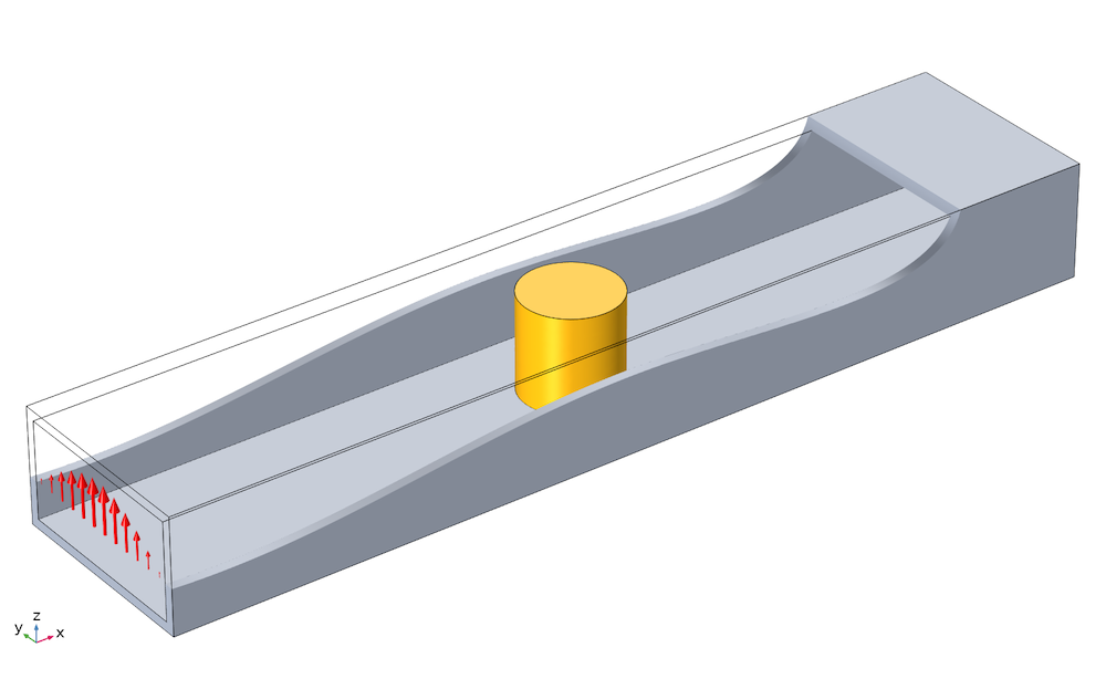
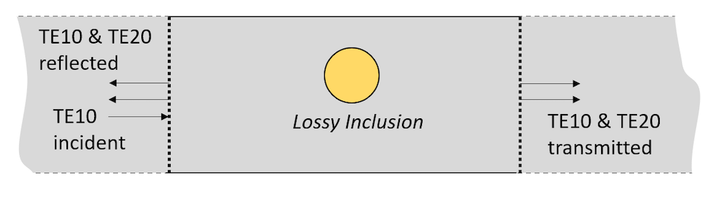
A rectangular waveguide excited with a TE10 mode and a lossy inclusion.
Assuming that the walls of our long rectangular waveguide can be modeled as lossless perfect electric conductors (an adequate approximation of reality), we know that the tangential component of the electric field must be zero, but the normal component of the electric field can be nonzero on the walls. Furthermore, let’s assume that the excitation (which we won’t be modeling) injects fields with the electric field polarized parallel to the shorter axis of the rectangular waveguide cross section. In the image above, this means that the electric field is polarized purely in the z direction, and the electromagnetic fields propagate solely in the xy-plane.
We will further restrict the discussion to a waveguide that does not go up or down in the z direction, but we will consider a single, off-centered, lossy inclusion within the waveguide that extends through the entire height of the interior that will reflect, and absorb, some of the guided signal.
Under those assumptions, it is valid to simplify our discussion to a 2D model, as shown below, of just a short section of the waveguide around the inclusion. We will start by addressing the case of a waveguide operating just a little bit above the first cutoff frequency of the TE10 mode. The correspondence between such a 2D model and a full 3D model is demonstrated in this example of an H-bend waveguide.
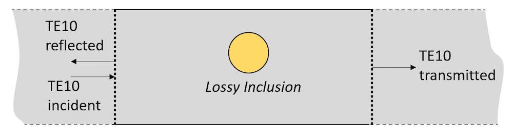
Schematic 2D waveguide model. The port at the left both launches a TE10 mode and monitors reflection, while the port at the right monitors transmission. There is some loss within the off-center inclusion due to finite material conductivity.
Such a model can be set up by drawing the geometry as shown, applying representative material properties, and using two Port boundary conditions — one at either end. The Port boundary condition imposes that the boundary is transparent to the specified mode, and also computes S-parameters when there is a single excited port.
The ports should be placed sufficiently far away from the inclusion such that the actual fields at that section of the waveguide are solely the guided modes, and not the evanescent component of the fields that will exist near the inclusion. It is unfortunately not possible to determine how far these evanescent fields extend, but a good rule of thumb is to place the port at least one-half wavelength away from any inclusions, and to study increasing this distance to see if this has any significant effect upon the results.
The settings for the excitation port are shown in the screenshot below. The only difference between the two ports is that, in the second port, Wave excitation at this port is set to Off.
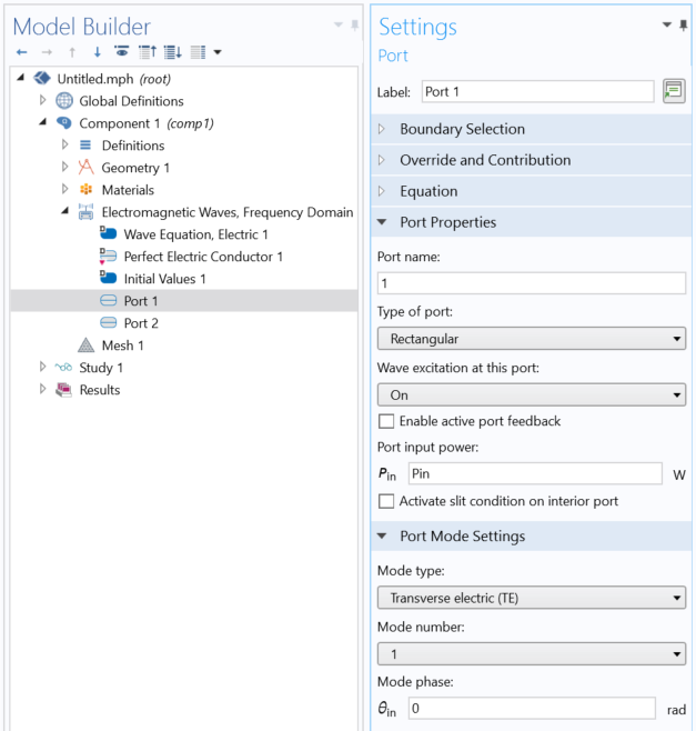
Relevant settings for exciting a 2D waveguide model with a rectangular mode.
Once we solve such a model, we can evaluate S-parameters, or we can integrate over the two port boundaries the power inflow/outflow. The sum of transmitted, reflected, and absorbed power within the inclusion should sum up the imposed power at the input port. If these integrals need to be computed very accurately, then a boundary layer mesh of one very thin element at the port boundaries is called for, as shown in the image below. This is only necessary for computing the power flow accurately; the S-parameter calculations are not as sensitive to the mesh.
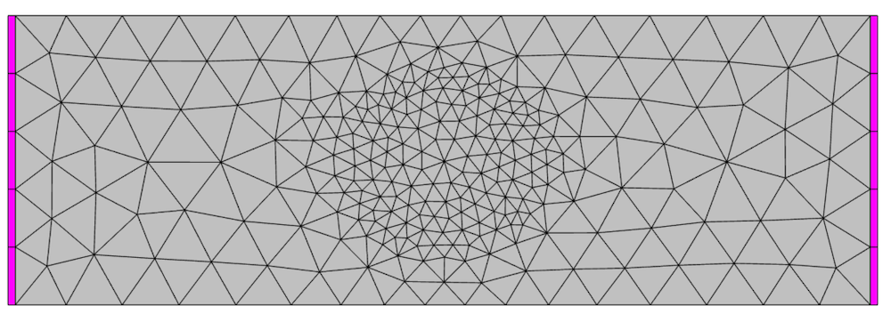
Mesh showing the single boundary layer mesh (magenta) at the two port boundaries.
Multiple Waveguide Modes at Higher Frequencies
As we increase the operating frequency high enough, we get to the point where the next highest supported mode, the TE20 mode, can exist within this waveguide. We are still injecting solely the TE10 mode, but the off-center inclusion will interact with the TE10 mode and cause conversion into higher-order TE20 modes that will be both reflected and transmitted.
At higher frequencies, the off-center inclusion causes scattering into higher-order modes.
Accounting for this situation is really quite simple. We just have to add two more Port boundary conditions, one at either end, that allow the TE20 mode to pass through and monitor the fraction of the signal that goes into this mode.
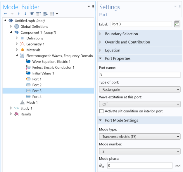
Settings for a port that monitors the TE20 mode.
Adding multiple Port boundary conditions to the same boundary is perfectly acceptable, and in fact necessary for correctness. If you do not do so, then the boundary will actually perfectly reflect any TE20 mode that propagates toward it, which would mean the results are incorrect.
You may already see a difficulty: If the frequency is so high that there are many possible modes, you would have to add a Port boundary condition for each one. This is not a big problem for this 2D rectangular waveguide with only two modes supported, but suppose you have a 3D circular waveguide? This supports many more modes and might be quite tedious to keep track of.
Let’s now look at a different approach for this case.
Truncating with a PML Rather than with Multiple Ports
Rather than truncating the modeling domain with several Port boundary conditions, you can also truncate the modeling domain with a perfectly matched layer (PML) domain, which can absorb almost any type of field very well, as discussed in this previous blog post. The model is extended a small bit on either side, with an additional PML domain that acts to absorb any fields that are incident upon it, regardless of mode. By adding this PML, we no longer need to add any ports, other than the port launching our mode of interest. We do, however, need to add additional boundaries at which to monitor the transmitted and reflected fields, as shown in the schematic below.
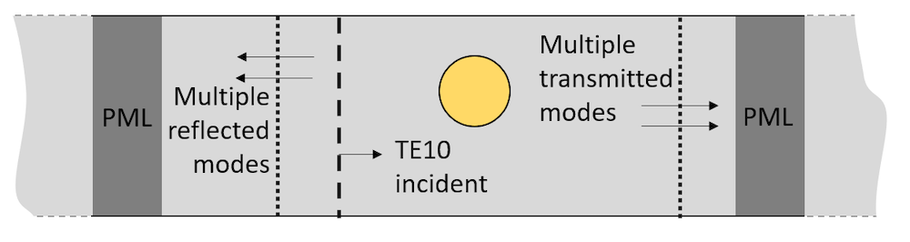
Schematic of model truncated with PMLs and using an interior port.
The launching port does also have to be treated in a special way. We need to launch the wave from inside of the modeling domain. This requires that you enable the Activate slit condition on interior port option. When this option is enabled, you can apply the port to an interior boundary, switch the Power Flow Direction, and set the Port type to be Domain-backed, meaning that any waves reflected back toward the port will propagate through it, and into the domain behind the port.
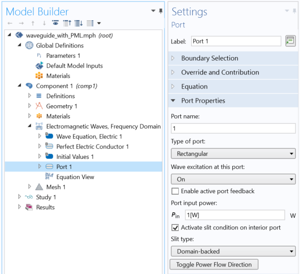
Settings for the interior domain-backed slit port.
Although we lose the ability to determine the fraction of energy reflected and transmitted into all of the different modes, we simplify our model setup by not having to account for each mode via a different boundary condition. If we are interested in finding just the transmission/reflection into one, or a few, of many modes, we could even combine the two approaches, adding interior slit ports to monitor only those modes of interest, since the PML will absorb all other modes.
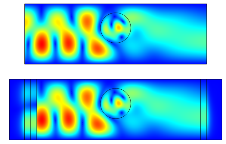
Results show agreement between these approaches of using multiple Ports (top) and a PML-truncated domain with a single interior Port (bottom).
The image above compares the results of the two approaches presented here, and shows agreement. This technique can be useful for any case where you have the possibility of multiple modes, or even other scattered fields, present at a boundary. The model developed here is also available via the link below.