A frequent modeling situation encountered in wave electromagnetics modeling is to compute the scattering of light off of a structure patterned on top of a uniform dielectric substrate. In this blog post, we will present one way to model such situations in the COMSOL Multiphysics® software.
Background and Overview
The case we will consider here is of a small scatterer of light: a half-cylinder of gold patterned on top of a dielectric substrate. We are interested in the case of just a single scatterer, and we will assume that the illumination is from a beam of collimated light that is so much larger in diameter than the scatterer, so that it can be well approximated as a plane wave. The plane wave can illuminate the structure at an arbitrary angle and state of polarization. The dielectric substrate is assumed to extend infinitely in the negative z direction.
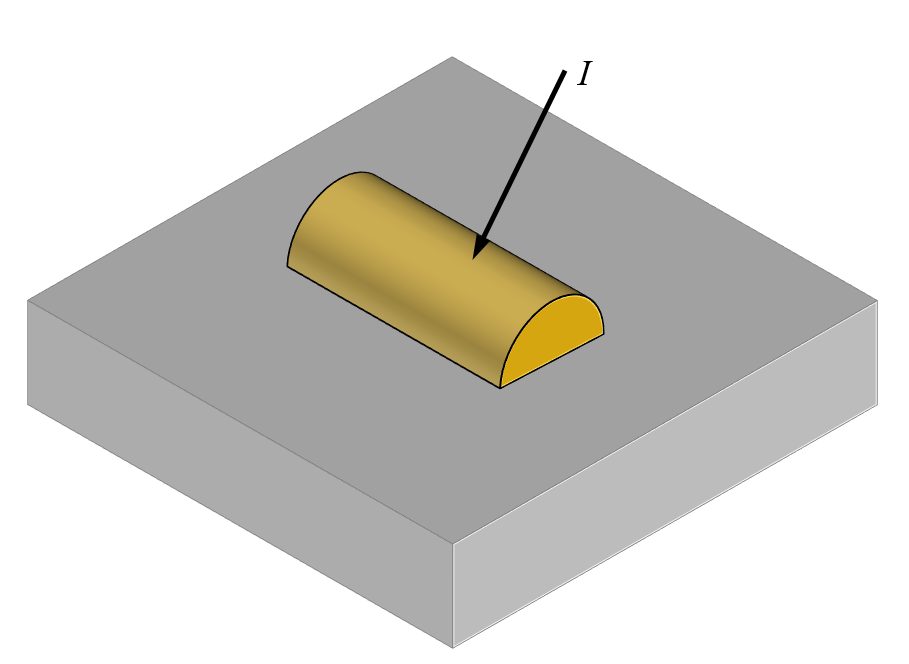
Light incident at an arbitrary angle on a single scatterer on a semi-infinite dielectric substrate.
Since we want to model just a single scatterer that represents a relatively small perturbation in a background field, it makes sense to use the Scattered Field formulation. This formulation requires that we enter a background electric field that would represent the solution to Maxwell’s equations in the absence of the scatterer. That is, we solve Maxwell’s equations in their frequency-domain form:
But write the total electric field as:
Rather than solving for the total field, we solve for the relative field, also often called the scattered field. The background electric field is the solution to Maxwell’s equations over the domains in question in the absence of the scatterer. For the simple case of an object in free space, the background field is simply a plane wave, as used in the RF Module benchmark example Computing the Radar Cross Section of a Perfectly Conducting Sphere, which compares the solution of this method against the analytic result. A similar example from the Wave Optics Module computes the scattering off of a gold nanosphere. One might be tempted to use the same approach for a dielectric half-space, but then the background field would be wrong.
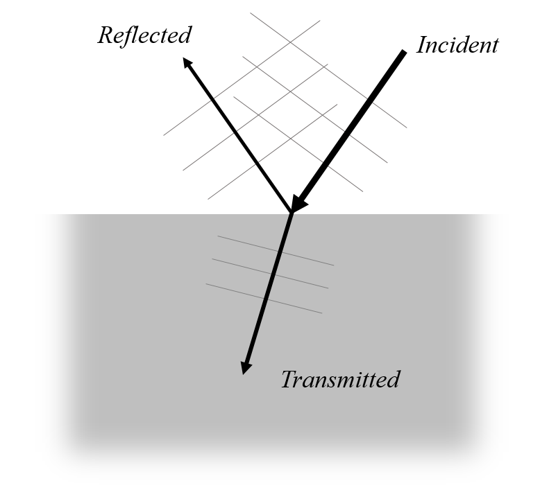
The electric field at a dielectric interface, absent any scatterer, is the sum of the incident, reflected, and transmitted plane waves.
For the case of a scatterer on a semi-infinite lossless dielectric substrate, the equation for the background field must incorporate the reflection and refraction at the interface. One approach is to compute the background field based upon a separate analysis and use that computed field as the background field. This approach is demonstrated in the Scatterer on Substrate example from the Application Gallery. However, here we will instead look at directly entering the background fields for a light incident upon a dielectric half-space by using the analytic solution.
Using the Fresnel Equations to Define the Background Field
The Fresnel equations, along with Snell’s law, describe the reflection and transmission of a plane wave of light when incident upon a flat interface between two materials of different refractive index. These Fresnel equations begin with the definition of the plane of incidence, which is a plane described by the vector normal to the surface between the two materials, and the wave vector of the incoming plane wave. The incident electric field can be decomposed into a component that is purely perpendicular to this plane, called an s-polarized or TE wave, and one that is purely parallel to this plane, called a p-polarized or TM wave. For example, circularly polarized light is the sum of a TE wave and TM wave of equal magnitude, but 90° out-of-phase with each other.
In the plane of incidence, we can use Snell’s law to relate the angle of the incident ( ) and transmitted (
 ) light relative to the surface normal in terms of the refractive indices,
  and
and  , of the two materials:
Then, the Fresnel equations give us the reflection and transmission coefficients for the TE- and TM-polarizations:
rr_{TE} = \frac{n_a \cos \theta_i – n_b \cos \theta_t}{n_a \cos \theta_i + n_b \cos \theta_t} \\
t_{TE} = \frac{2 n_a \cos \theta_i}{n_a \cos \theta_i + n_b \cos \theta_t} \\
r_{TM} = \frac{n_b \cos \theta_i – n_a \cos \theta_t}{n_b \cos \theta_i + n_a \cos \theta_t} \\
t_{TM} = \frac{ 2 n_a \cos \theta_i }{n_b \cos \theta_i + n_a \cos \theta_t}
\end{array}
The TE- and TM-polarized components of the incident plane wave have to be transformed from the plane of incidence back to the global Cartesian coordinates.
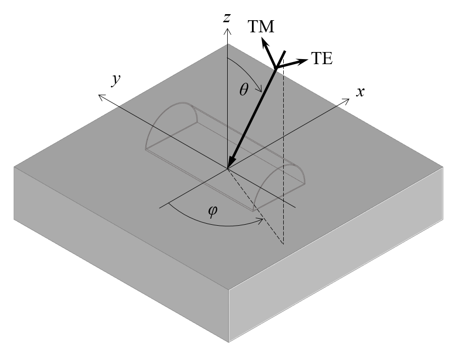
We must next transform these from the plane of incidence back into the global Cartesian coordinates to get the k-vector of the incident and transmitted beam. Following the convention that the plane of the interface is the xy-plane, and the incident beam of wavelength  is propagating in the negative z direction, we define the angle of incidence
  as the angle from the z-axis, and the angle
  as the rotation about the z-axis starting from the negative x-axis, as shown in the figure above. This lets us define the k-vectors of the incident beam as:
And the transmitted beam:
The k-vector of the reflected beam,  , is similar to the incident beam, but of opposite sign for the z-component.
Given an incident beam that is composed of both a TE- and TM-polarized component,  and
and  , the components of the electric field of the incident beam are:
And for the reflected components:
So, the total background field on the incident side is  , and of the other side of the interface, the field is
  , with components:
These expressions can be entered as sets of variables defined over different domains within the COMSOL Multiphysics® software, and used as the background field definition.
Sample Model and Discussion for Modeling the Scattering of Light
A sample model demonstrating this approach is set up and available via the link below. The electric field magnitude and the losses in a small half-cylinder of gold are plotted.
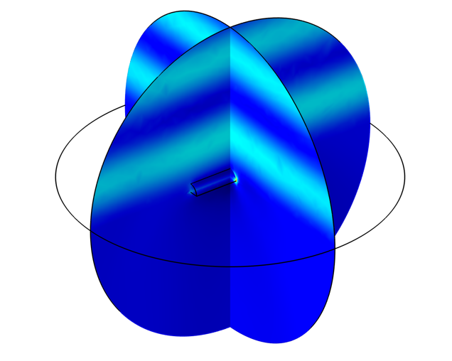
Electric field magnitude around a gold scatterer on a dielectric substrate.
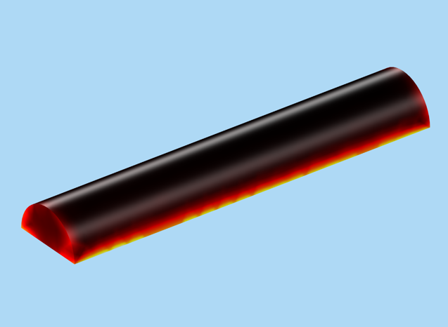
Losses in the gold scatterer.
Although this approach of entering the analytic background field is a little bit more work in terms of model setup, it is faster to run than the Scatterer on Substrate example, which first has to compute the background field. The merits of the latter approach would be when considering a case where the analytic solution is more difficult, or even impossible, to write out. So, for the case of a uniform dielectric substrate, this approach is likely always preferable.
Next Step
Try modeling a scatterer on a substrate using the analytic background field by clicking the button below. Note that you must be logged into a COMSOL Access account with a valid software license to download the MPH-file.